Using a Logic Analyzer
If you ever worked with a logic analyzer you know: The logic analyzer is one of the most valuable tools for troubleshooting. In principle, a logic analyzer is a fairly simple device. It simply records the states (i.e. logical 0 or 1, or more precise, low and high) of a number of digital signals for later analysis. So you can, for example, check whether a single signal ever changes during a certain operation, or you can record full system bus or processor activity, depending on where the analyzer is listening.
About Logic Analyzers
For recording logical states of certain signals, it has to be established electrical contact to those signals. This is done by so-called 'probes', which can be directly attached to the pins of the chips you are observing. Sometimes you might have to use a suitable physical connector (e.g. when checking interfaces) for connecting those probes. The number of probes required depends on the number of signals you need to observe.
For the logic analyzer, all signals are recognized as 'input channels'. The maximum number of input channels which can be recorded is one of the main characteristics of every logic analyzer. Typical values range from eight to 64 channels in steps of eight. The combination of the states of all channels at a certain point of time is called 'sample', and the process of recording those states on a time line is called 'sampling'. Another feature of a logic analyzer is the minimum timing resolution, or granularity, which can be selected for sampling the signal states. This minimum timing resolution will define the maximum signal clock rate, which can be safely sampled (sampling rate should be at least twice the signal clock). Finally, the number of recorded samples is limited by the sampling memory which is implemented inside the logic analyzer, at least as long as the sampling rate is above what you can securely stream to mass storage.
Now, why are logic analyzers so useful for troubleshooting? Main reason is that everything what happens inside a computer is happening lightning fast in real time. Including bugs and errors. And different to a code debugger, you in general can't step through the system operation by simply stopping and releasing the run of the system. So, record system operation in real time, and do the analysis afterwards. And this is exactly what the logic analyzer provides.
In fact, some effects can only be diagnosed by using a logic analyzer. Bus failure belongs to those effects, and protocol errors, sometimes too. Especially if the whole system refuses to work although all supply voltages are ok, a logic analyzer often is the only choice for isolating the cause by tracing what's going on.
All logic analyzers need a message when to start recording samples, so that the action of interest will be captured properly. Doing this manually normally won't work, since so many events have to be captured in such a short time, that the sampling memory will be filled before the point of interest ist reached. So there are automatic means for starting with recording which are called 'triggers'. A trigger normally is defined by a rule, which describes the condition which has to be met in order to start sampling. This can in general be a change of a single signal, or a defined combination of states of multiple signals, or a special sequence of a defined combination of mutiple signal states. In theory, there are no limits on how to define a trigger with a rule. Practically, logic analyzers can't process rules beyond a certain complexity because the trigger has to be evaluated in real time.
Last, but not least, it has to be defined, once a trigger has been fired, at what time distances the signal states are being captured as samples. Digital circuits like a computer normally have defined state cycles, which are controlled by a system clock. So normally it is a good idea to couple the sampling clock with the system clock of the tested object. Sometimes it is not the system clock, but another bus signal which better defines the points in time where the signal state should be recorded. For example fo capturing I/O data, it might be useful to use a data valid signal as sampling clock rather then the system clock. Direct advantage of sampling only the states of interest is that the overall recording period can be longer with respect to the always limited sampling memory. However it can happen, that no useful clock reference is available, in which case an internal clock can be used by the logic analyzer to sample signal states continuously in equal time slices.
Which One to Choose
Now that we know about samples, triggers and clocks, and we have learned how useful a logic analyzer can be, what would be a suitable logic analyzer for troubleshooting a 9845?
Probably the main requirement is that the logic analyzer is capable on keeping up with the 9845 system clock, which is 5.7 MHz. So the logic analyzer should be capable to sample at least 12 million samples per second for capturing all system states during normal operation. However, if there is a timing problem which has to ba analyzed, or 'glitches' during state changes of signals, the sampling frequency should be a multiple of this, with recommended >100 million samples per second.
Concerning the size of the sampling memory, there in general is only one rule, it should be as large as possible. Older systems often start at 2k samples, but more is always better, especially for program debugging (more to this later on this page).
The number of channels needed depends on what has to be diagnosed. If you need to capture all signals of a system bus like the 9845's IDA bus or the I/O bus at once, you would need 34 channels. Recording all test connector signals of a PPU at once would require 40 channels. However for most applications, 32 channels would be ok. 16 channels on the other side would allow tracing control lines or I/O like HP-IB, but again this would not be enough for program debugging. So a 32 channel logic analyzer would be recommended.
All logical signals in a 9845 have TTL level. Which again means that all channels have to be at least 5V tolerant (with some headroom above) and have to safely set a threshold on the TTL definitions on logical low (< 0.8V) and high (> 2.0V). This differs from today's computers logic voltages, which nominally in most cases work at 3.3V and below. There also should be an external 5V tolerable clock input with its thresholds on the proper TTL logic levels.
Finally, any kind of interface is useful to transfer the sampling data from the logic analyzer to the PC for further analysis processing. Best suited of course is a USB interface, but in principle any other kind of interface (RS232, HP-IB, whatever) will do it. And don't forget that the hardware is only half of the solution, there should be a capable software for supporting the necessary analysis.
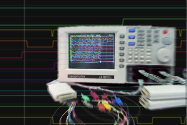
The market for logic analyzers is manifold and as old as the HP 9845 itself and offers a wide range of models. If you don't already own one and are looking for a budget solution, you can consider a used older one from ebay. Especially if you primarily want to use it for vintage computer troubleshooting. Also certainly good choice is a simple but ingenious solution, the Open Logic Sniffer (OLS), which is based on an FPGA programmed for logic analyzer tasks (a solution originally introduced with Michael Poppitz' SUMP project).
The Open Logic Sniffer (OLS)
You don't necessarily have to acquire a full-fledged logic analyzer for troubleshooting a vintage computer system. All system signals usually are below 10 MHz, and complex analysis is much more a matter of software than a hardware issue. So from my own point of view, concerning hardware, less is more. Or in other words, use as much hardware as needed for sampling with the required quality, and if ever possible use standard hardware which is produced in high quantities, and then use the software (ideally running on a PC) for doing everything else (including controlling the hardware and doing the analysis). In fact this also goes along with the demand for a budget solution.
There are different solutions how to achieve this minimum hardware approach. Most common are those based on microcontrollers (such as AVR or PIC) or FPGAs/CLPDs. In principle you can just add the proper firmware for recording samples and some buffers for decoupling input channels and chip inputs, and then use the built-in RS232 or USB interface for controlling the sampling operation and for data transfer to the PC, where a software client does the remaining work.
It seems that FPGAs are probably the best solution, since they allow higher sampling rates of up to 200 MHz. The most prominent FPGA example probably is the SUMP project, where a standard Xilinx Spartan 3 Starter Kit Board is used as hardware base for a logic analyzer. Basically, there had to be developed the proper firmware and a PC software client. Since the results of this project are open source, there are derivates like the Open Logic Sniffer, which continue the development on this approach.
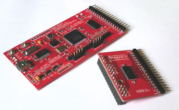
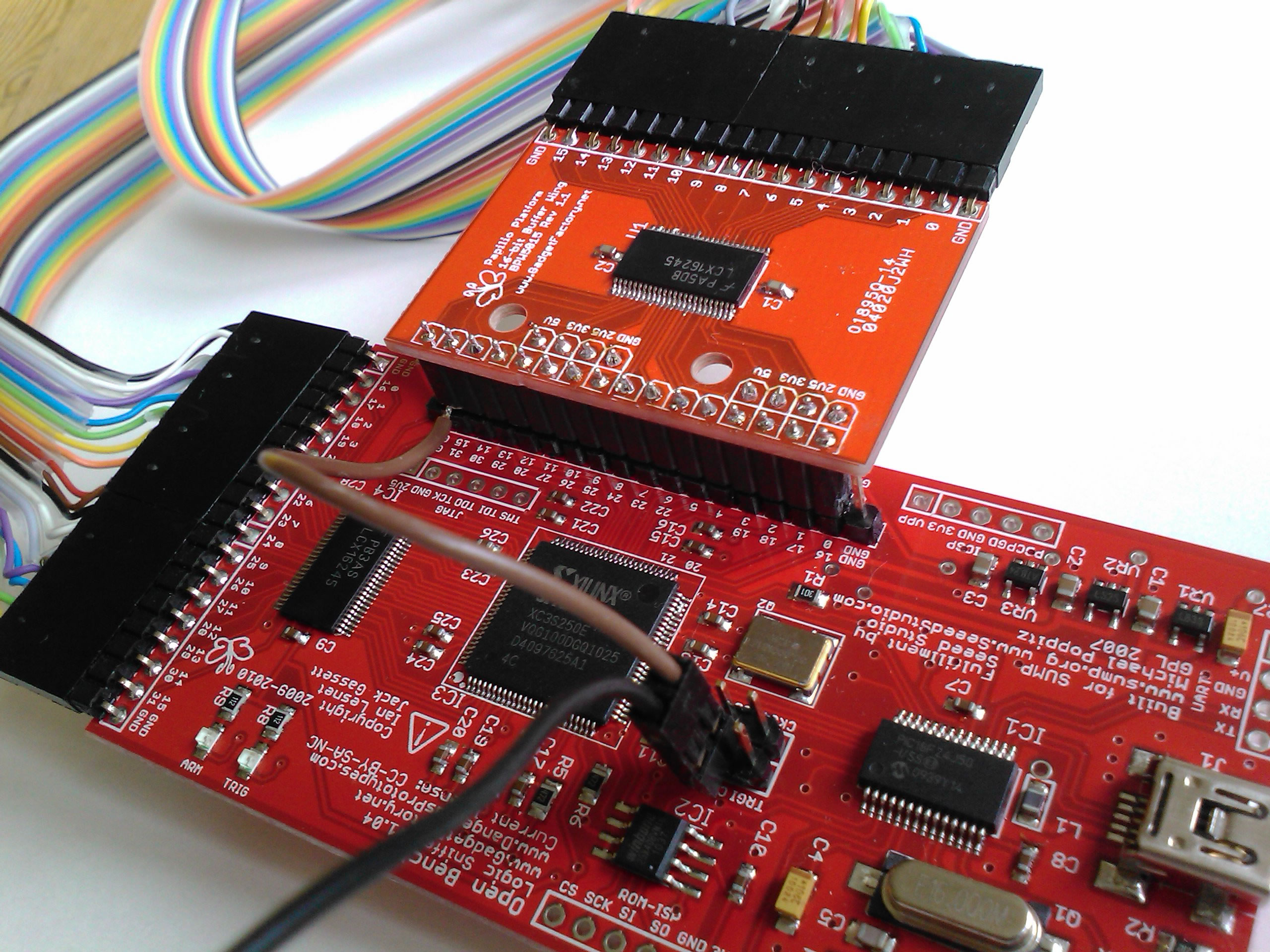
Open Logic Sniffer with 16-Bit Input Wing
The Open Logic Sniffer - a joint project of Gadet Factory and Dangerous Prototypes - features up to 200M samples per second, 16 5V tolerant channels plus 16 direct input/output channels, 16k 8-bit and 4k 32-bit sample memory, internal/external clock and trigger and USB interface, this all for USD 50 (see Seeed Studio for selling the ready-to-use OLS with worldwide shipping). I strongly recommend also to order the 16-bit Input Wing as needed for taking full advantage of the 32 channels on TTL signals (e.g. for program debugging). There are several variants for the client software available, I got good experience with Jan Willem Janssen's Alternative OLS Client (see this link for Jan Willem's site). The analyzer client software is open source, offers a plugin interface and can be tailored to special 9845 tasks.
All examples below refer to a OLS with Input Wing extension and Alternative OLS Client software.
How to Connect to the HP 9845
Once you tell a logic analyzer your own, the next question is what to sample, and where to connect the probes. The subject for sampling of course depends on what kind of information you like to collect. However there are two connection points which I would recommend to take into consideration. For the 9845B/C there are so-called test connectors on the top of both the LPU and the PPU processor/memory controller boards (A15/09845-66515 and A16/09845-66516), which provide convenient access to the most important processor signals. Probably those connectors once have been used at HP to perform the factory testing.
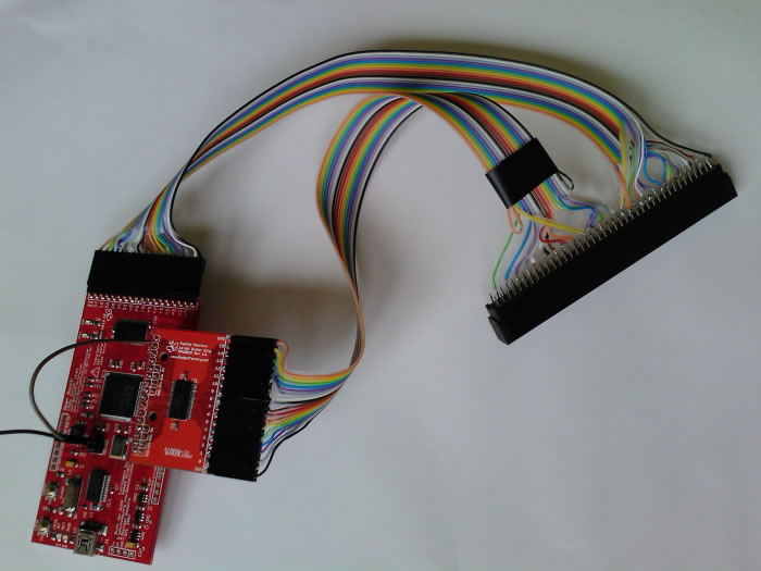
OLS Example Setup for Connecting to the Test Connector (with Input Wing)
The pinout of those connectors is as shown in the following diagram:
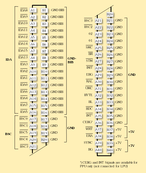
Test Connector Pinout (9845B/C LPU & PPU Processor Boards)
Note that the test connectors are available for the A15 (LMC) and A16 (PMC) assemblies only. The bit slice LPU processor of the HP 9845 Model 200 systems features another type of test connector, which can't be used for tracing system operation as described here.
Those connectors can be accessed with a standard edge connector plug with 2x40 contacts (2.54 mm raster). All you have to do is to assemble a suitable ribbon cable with the edge connector at one end and pin connectors at the other end. Deviating from the above photograph I would recommend mounting an IDC connector to the ribbon cable and building an adaptor from the IDC connector to the edge connector (e.g. by soldering the edge connector on a lean PCB) to prevent possible short circuits. The pinout again depends on what you like to do (since with 32 channels at least for the PPU not all signals can be captured at once), but in general I would recommend the following connections:
Standard OLS connector |
Input Wing connector |
|||||
Channel |
Test Connector |
Signal |
Channel |
Test Connector |
Signal |
|
0 |
A12 |
IDA0/ |
16 |
A17 |
BSC0/ |
|
1 |
A11 |
IDA1/ |
17 |
A18 |
BSC1/ |
|
2 |
A10 |
IDA2/ |
18 |
A19 |
BSC2/ |
|
3 |
A9 |
IDA3/ |
19 |
A20 |
BSC3/ |
|
4 |
A14 |
IDA4/ |
20 |
A21 |
BSC4/ |
|
5 |
A16 |
IDA5/ |
21 |
A22 |
BSC5/ |
|
6 |
A13 |
IDA6/ |
22 |
A25 |
SMC/ |
|
7 |
A15 |
IDA7/ |
23 |
A27 |
STM/ |
|
8 |
A1 |
IDA8/ |
24 |
A28 |
INIT/ |
|
9 |
A2 |
IDA9/ |
25 |
A29 |
EBG |
|
10 |
A3 |
IDA10/ |
26 |
A32 |
BYTE |
|
11 |
A4 |
IDA11/ |
27 |
A33 |
BL |
|
12 |
A5 |
IDA12/ |
28 |
A35 |
INT/* |
|
13 |
A8 |
IDA13/ |
29 |
A37 |
WRT/ |
|
14 |
A6 |
IDA14/ |
30 |
A39 |
SYNC |
|
15 |
A7 |
IDA15/ |
31 |
A23 |
02 |
|
*) The INT/ signal is available at the PPU test connector only.
With this setup, you have full addressing & data access (including block select codes), you can safely decode all memory handshakes, and separate all types of memory access (including bus grants) and finally trigger to system reset and I/O interrupts.
Note that one side of the test connector holds all signals, and the other side voltages and grounds. You should connect one of the the OLS ground inputs to one of the test connector (e.g. to pin B1).
Important: Once the OLS is connected to the 9845 test connector in this way, you should thoroughly check whether the orientation of the edge connector is correct, otherwise you would connect the GND and supply voltage contacs to the OLS inputs. There is not keying for the edge connector.
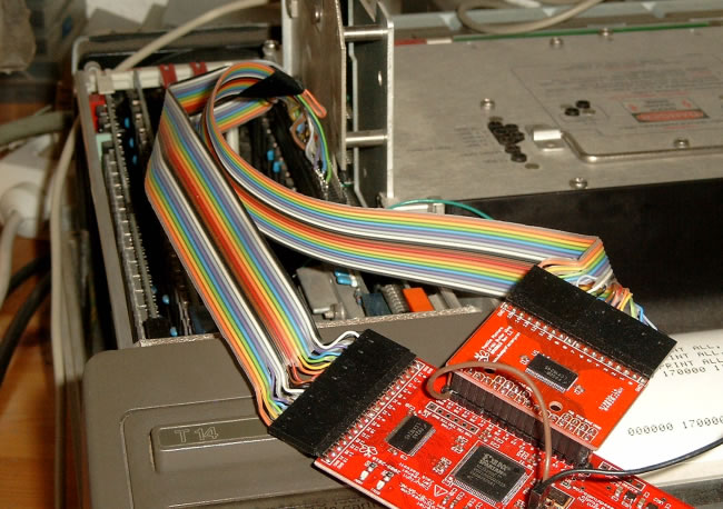
Routing the External Clock Input via Wing Channel 31 (Click to Enlarge)
There are two complementary clock signals (01 and 02) provided at the test connector which can be used as external clock signal for the analyzer (it doesn't really matter which one you use, I am using the rising edge of 02 as external clock input). You have to take into account that the external clock input of the OLS is not TTL tolerant, so you should route the external clock signal from the 9845 via the Input Wing's buffer in order not to overstrain the OLS' external clock input. In the above photograph, channel 31 of the Input Wing (which itself is connected to the 02 signal of the test connector at the 9845 side) is connected with the brown cable to the External Clock Input pin of the OLS board (please ignore the black cable which is of no use here).
OLS with Adapter Mounted to PPU
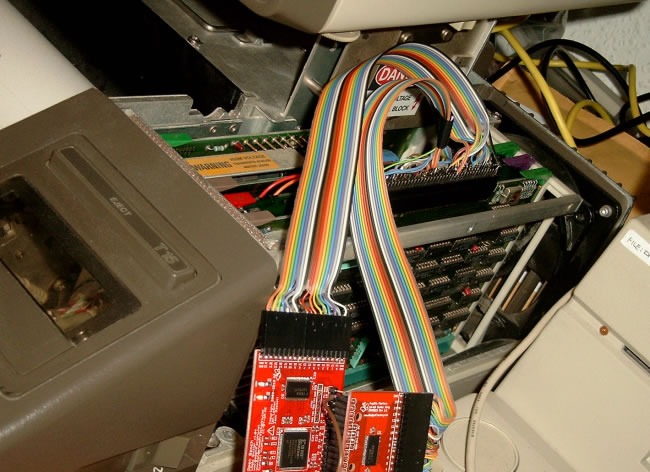
OLS with Adapter Mounted to LPU
Using the OLS Client Software
Before using the OLS client software, you have to download the latest version it from Jan Willem Janssen's web site. My Asm45 plugin should be already included. If not, you can download it from the downloads section at the end of this page and save it into the client's plugins directory. For Windows it will be necessary to also install a driver from the original OLS downloads page (see this link). Linux should work out-of-the-box.
Using the OLS client software is pretty straight-forward. Once you started the software with run.bat under Windows or 'sh run.sh' under linux , you see the (yet empty) analyzer worksheet with a menu bar above. First thing you should do is configuring your project. You also can load a pre-configured setup, which I would recommend if sampling from the test connector (there is a project template called 9845-test-connector.olp included in the Asm45 plugin's distribution package).
All settings for the communication between the software client and the OLS hardware ("Connection"), for sampling ("Acquisition") and for trigger rules ("Triggers") are can be accessed via the Capture menu under the "Begin capture" entry. The Acquistion setting should be selected as follows:
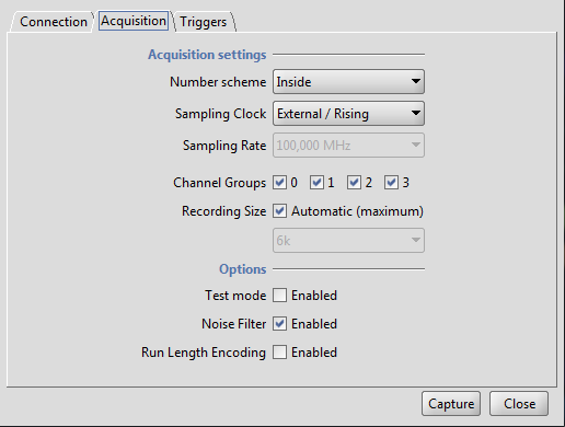
Recommended Settings for Acquisition via Test Connector
You can also customize the signal analysis display by changing the Diagram settings (e.g. redefine the channel labels).
Another important control for the sampling process is the Triggers dialog. You can completely disable any trigger, which tells the OLS just to start sampling when the Capture button is clicked until the sampling memory is filled up. If you need to wait for a certain event, you have to set a trigger. With the OLS client, you can do this with a simple (one-stage) trigger or with a complex (multi-stage) trigger.
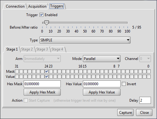
Example Trigger Settings
In general a "simple" trigger profile is ok. The trigger mask defines the signals which are involved in the trigger, and the value which type of event fires the trigger when detected by the OLS hardware. See the above example for setting a trigger to the point where the INIT/ signal (bit 24) gets logical high, which indicates that the system initialization phase is complete and system ROM execution can start. For my own convenience I have slightly modified the original client code so I can specify trigger mask and values also as hexadecimal numbers, including inverted (= negative-true logic) if applicable.
The before/after ratio defines the window for the samples recorded before the trigger and after the trigger. This is possible because in fact the OLS is recording samples all the time, and it simply trashes all sampling values which are before and after the defined sampling windows.
After clicking the Capture button, the OLS immediately starts sampling. If a trigger is set, it waits for it before remembering the sampling data into the sampling memory until the sampling buffer is full, which automatically stops the sampling process. After this the sampling data is shown on the analyzer worksheet as signal / time diagram with color coded channels. You then can zoom into the worksheet or set markers, save the sample data to disk and much more.
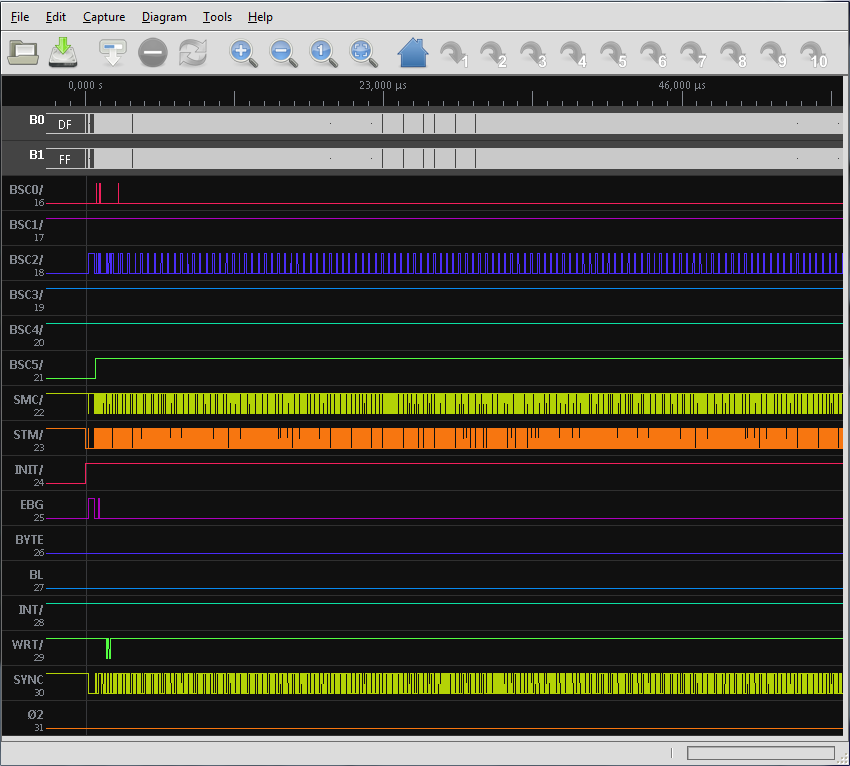
PPU System Startup, Viewed from the Test Connector (Overview)
See the example screenshot above, which combines channels 0-15 as decoded data words, and shows all other signals as logic diagram. Note the trigger is set at the point, where the INIT/ signal changes from low to high. You can now zoom into the diagram to see what's happening in detail when system control is transferred to the PPU ROM:
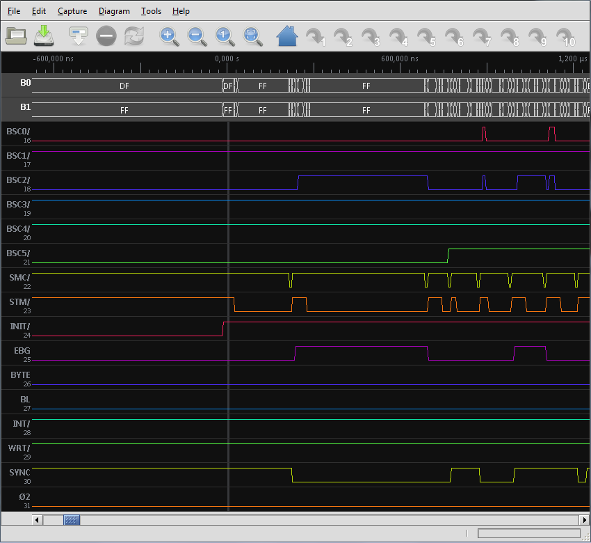
PPU System Startup, Viewed from the Test Connector (Zoom)
But most interesting is the plugins palette, which can be accessed via the "Tools" menu entry. There is an submenu entry for each plugin which is present in the plugins directory of the OLS software. Including the Asm45 bus analyser plugin, if copied to this directory.
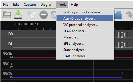
OLS Client Plugins Menu
The Asm45 OLS Plugin
But the OLS can do more. As mentioned above, the OLS client can be easily extended with prebuilt plugins. Plugins are processors, which interpret the recorded sampling data for getting "cooked" information out of it. There are already a number of plugins as part of the OLS client distribution, such as an I2C or JTAG analyzer. In principle they all do the same: They analyse the sampling data by adding meaning to the signals, by getting the singnals into relation with each other and by detecting the protocol events which ar formed by the signals. This high level data then is presented to the user so that he or she has no longer to cope with low level signal information, but with what the samples really tell what is going on.
For the HP 9845 it means, with the right plugin you can trace the commands and the data which are happening on the bus. Great?
Now when looking for example at the 9845 IDA (data & address bus) you in principle can peek the address, data and machine instructions, which are passing this bus. Which again would give an inestimable tool for directly tracing code execution. And this is exactly what I have written an own plugin for. It is called Asm45 plugin since it extracts all address, data and instruction information which is going over the bus, and presents this data as disassembly to the user. If you now compare this run-time disassembly with the static disassembly e.g. of the system ROM, you get an idea how the system works the ROM code, and if there is a problem, where it might be located.
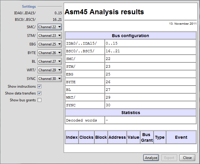
Asm45 Plugin View
Als you can see in the Asm45 plugin view, you can set the bus signals to the channels as you like. The default setting reflects the test connector mapping as shown in the connector table above. IDA and BSC signals are strictly bound to input channels 0 to 15 and 16 to 21, respectively. Depending on your control line setup, you can assign the other channels as needed. Also you can select whether instruction execution, data transfers within the execution of an instruction, or bus grants (i.e. DMA) like the CRT memory cycle 'stealing' shall be included in the analysis.
Click the Analyze button to achive an assembly output like the following:
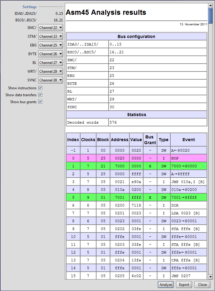
Asm45 Plugin Analysis View
The analysis starts with a short report of the current channel assignment and the number of instruction or data words analyzed (typically there is a ratio of ~1:5 for samples vs. decoded words).
Index simply marks the word count starting at the trigger point with 0. Clocks gives an idea how many system clocks were needed to execute the operation (not fully accurate in every case), Block shows the memory block which has been involved and Address the address within this block, both in hexadecimal notation. Value is the recording of the IDA0..IDA15 lines (again hexadecimal), Bus Grant tells whether the action belongs to a DMA transfer, and Type shows whether the action is an instruction (I), a 16-bit data word access (DW), an 8-bit data low byte access (DBL) or an 8-bit data high byte access (DBH). Event shows the decoded action. Arrows mark the direction of data transfers (to or from memory) with memory address always left and data value right of the arrow. See the 9845 Assembler Project Section for more information on the 9845 Assembler.
Note that the trigger is indicated by a light magenta background. Instructions have white background, whereas data transfers are marked with light blue background, and DMA transfers with green background. Use the filter checkboxes to include/exclude information not required. Adresses in brackets usually represent calculated absolute addresses derived from an relative address included in the instruction. [B] indicates that a base page memory access is involved.
You can use the Export button to save the result either as HTML or CSV file.
What you can learn from the above example, is that the PPU starts execution at address 0020 in block 25 (step 0), the test ROM block. If no ROM code is found there (this is the case in our example), execution proceeds with address 0021 in block 5 (steps 3 + 4), where an indirect jump to address 0200 in the same memory block is executed. Then first of all interrupts are disabled with the DIR command, and so on. Note that immediately after checking address 0020 in block 25, execution is stopped for a DMA access to address 7000 in block 1 (block 21 is shown due to some glitch when decoding DMA block addresses), which is the CRT alpha memory where the alpha control logic is performing some 'memory cycle stealing' via DMA to get its display data. The second access to CRT alpha memory then is performed shortly after in step 5 (now with the correct block address). Going further in the analysis, you now can trace the complete startup procedure.
Tracing at a Selected Memory Address
Setting the proper trigger for execution traces can get a bit more difficult than simply setting a trigger to a single signal. Normally, for setting a trigger on a special execution memory block and address, I would recommend using 40BFFFFF as trigger mask. Then enter the memory block BB and execution address AAAA for which you want to record execution as inverted hex value of the form BBAAAA.
Note that with bit 30 set in the trigger mask enables checking the SYNC signal (which separates instructions from data) so that possible triggers caused by data transfers are ignored, and bit 23 (STM/) ensures that it really is address information which is read from the bus (and no temporary data). This works in most cases ok. However, you should always check in the plugin whether the trigger did work as expected, or whether the trigger has been fired by some other event, which you didn't want to trace.
As an example, we like to know what is happening at the point where PPU and LPU both execute the same code and try to figure out which is the LPU, and which is the PPU. We know (from the disassembly of the PPU system ROM), that this is done at hexadecimal address 0207 in block 5. So we're setting a trigger to this memory block and address by typing block 5 and address 0207 as 50207 into the "Hex Value" field. Then we check "Inverse" (because the IDA bus is using invert logic) and click "Apply Hex Value". Now we set the trigger mask in the "Hex Mask" field to include both block and address information and to check SYNC and STM/ to 40bfffff and click "Apply Hex Mask":
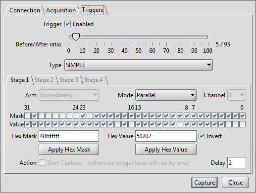
Setting a Trigger to Exceution Block and Address
Then we click the Capture button and switch the 9845 on. As a result of the following capture process, the Asm45 plugin then provides us with the following analysis, which tells us that at address 0207 (the pink row) there is a check for the vertical retrace signal (which is the same as the HLT signal), which - because vertical retrace is currently not in progress and HLT/ is logical 0 - does a branch to address 0211 in order to proceed as PPU at address 7A1E still within memory block 5:
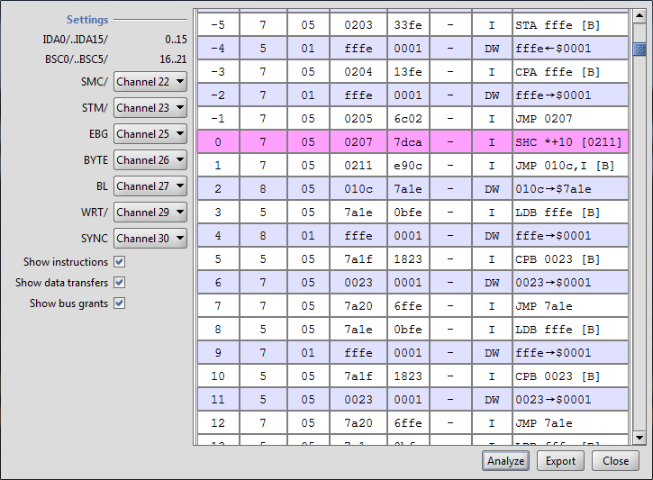
Asm45 Plugin View for Execution Trigger on Block 5 & Address 0207
If we would now connect the logic analyzer to the test connector on the LPU processor board, we would find a different behavior, since the HLT/ signal will always be logical 1 (HLT/ is grounded for the LPU), so that the LPU will try again, and when then finding HLT/ still being logical 1, it can be sure it is the LPU. It then changes execution to memory block 3, and jumps into its LPU initialization routine. It is as simple as that.
The same procedure can of course also be used to debug execution of programs in RAM, such as binary programs.
The OLS2Asm Program
The functionality of the Asm45 plugin translating the samples into meaningful assembler code is also provided by a console application ols2asm.exe which does exactly the same job on OLS sample data files (those files with extension .ols that are produced when saving sample data from within the OLS client). When run with an OLS data file as parameter, the OLS2Asm application does all necessary analysis and produces a text file with 9845 assembler output.
You can choose between different levels of detail: addresses & instructions only (this is the default), or with data (-v1), DMA (-v2), or with all recorded bus signals included (-v3). Execute ols2asm.exe without parameters to get an usage overview.
Note that the address/data information in channels 0-15 supplied by the ols2asm program output already has been converted from negative true logic to normal logic for convenience reasons, which is NOT the case for channels 16-32, which reflect exactly the signal levels as recorded.
Downloads
Click here for downloading alle items referenced in this tutorial:
| Asm45 Plugin Package for the OLS client software (also includes the OLS2Asm program): | asm45-ols-plugin-10.zip |
These first versions may still have bugs. Please use the contact feature to let me know if something doesn't work as expected.
See http://www.lxtreme.nl/ols for downloading the OLS Client for the Open Sniffer Board. Also can be downloaded from Dangerous Prototypes via this link (downloads seem to be currently broken). Sources are also available from github (see https://github.com/jawi/ols).
More Information
The most comprehensive source for the A15/A16 test connectors are the original schematics. See the documents section for Magazines, Patents & Schematics for downloading these references.