The 9845 System Architecture
As with most von-Neumann computers (and even today there is no basic change), the 9845 systems consist of central processing units, read-only memory for firmware, read-write memory for programs and data, a mass storage concept, keyboard and pointing devices for input, CRT, printers and plotters for output, and finally communication connections with peripheral devices and other computer systems.
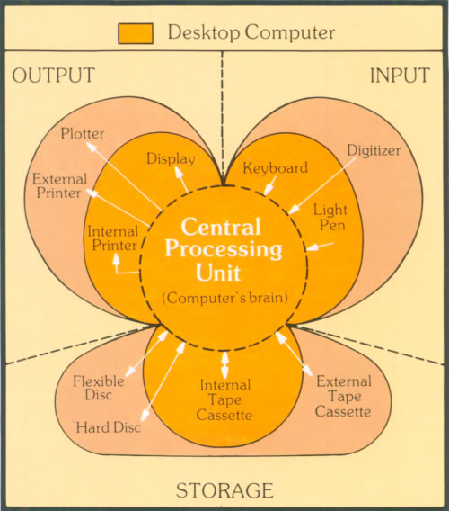
What made the 9845 series something special, was that, on one hand, it was the first time that such a high-performance integrated system was developed for the desktop, and on the other, there were design principles created and applied, which were exemplary for later desktop systems, and, in particular, so-called workstations.
The 9845 systems are completely based on a 16-bit architecture. Processors, system bus, I/O bus and all memory was designed for processing data with full 16-bit word width. In order to assure efficient processing of byte-oriented data like ASCII text or peripheral data, processing could be switched to byte mode for some stack operations.
Like the software architecture, the system architecture was not completely new. Many components and concepts had been derived from earlier designs (e.g. from the 9825) and simply adjusted for use in the 9845 systems. In contrast to other well-known computer designs, the 9845 design is actually a hybrid, merging the experiences and philosophies from two worlds, the minicomputer development and the desktop calculator development (and actually the know-how from two separate HP divisions, the minicomputer division in California and the calculator division in Loveland, Colorado). One of the curious things is that the 9845 can be used as calculator even while a program is running.
The Processors
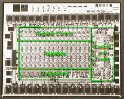
All 9845 were controlled by two processors working in parallel. One processor, the peripheral processing unit or PPU was responsible for all the I/O processing, like serving keyboard interrupts, writing data to the CRT display, or handling other peripheral I/O. The logical processing unit or LPU did execute all user programs, including BASIC programs and binary software modules.
For most systems, both processors were almost identical. The processor design went back on a very early minicomputer design, that of HP's first computer ever, the 2116A, which was transferred into a microprocessor design. So, much of the existing know-how and development environment of the 211x series could be recycled for the new processors. In fact, those processors were the first 16-bit microprocessors ever (as well as the 2116A had been one of the first 16-bit minicomputers before). Later HP introduced a modified high-performance version of the LPU, which was built on a custom bit-slice processor design, but still physically and electronically compatible to the original processors - the "hybrid processors".
The 9845 16-bit architecture is based on a big-endian byte order, so the most significant byte is stored first (same as the Motorola processors, but different to the Intel processors).
For more information on the 9845 processors please have a look at the Processors section.
The Memory
The 9845 series already used DRAMs as R/W memory and ROMs for the firmware. One design decision was to realize a complete operating system including BASIC development and runtime enviroment in firmware. As a result, the whole system was almost immediately ready to use after power-up.
Memory Organization
The directly accessable address space for the processor is 16 bit or 65,536 words. The processor supports different addressing modes, including indirect addressing (which covers the whole 64K address space), current page addressing (which provides direct addressing within a 1K window around the current program counter) and base page addressing (which is used to access the 1K page around address 0). Those addressing schemes probably need some explanation.
The current page addressing is the normal addressing. Most references within a program are located within a certain range around the current program counter. The processor designers decided that a window of 1K words should be OK. Since this relative address can be coded with 10 bits directly into the instruction, this addressing scheme is quite efficient and also sufficient for most cases. The 10 bit address is interpreted as a signed value between -512 and +511 and just added to the current program counter.
The base page addressing works identical to the page addressing with the speciality that the 10 bit address is not added to the current program counter but to the address 0. Resulting negative values are wrapped on the address space and so access the memory area from octal 177000 to 177777. The complete base page includes the memory areas 177000 to 177777 and 0 to 777.
The indirect addressing is used for all cases, where a certain memory location can't be accessed through the two other methods above. The address in the instruction refers to a 16-bit vector, which must be located within the current page. The content of this vector is now used as the final address, which can be anywhere inside the 16-bit address space. It needs more time (since the indirect addressing has to be resolved) and space (since the address is held in an extra 16-bit word) for execution.
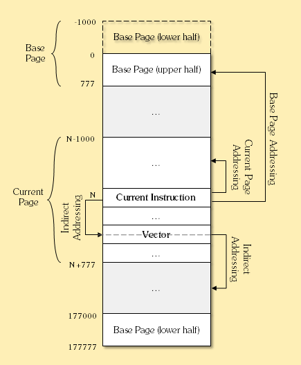
Addressing Modes of the 9845 Processor (N denotes the current program pointer)
Since most instructions fitted into one single 16-bit word including the address operand, the 9845 machine code wasn't much larger than the code of popular 8-bit microprocessors like the MOS 6502 or the Z80. And byte strings could be efficiently packed and processed anyway. Besides the benefit that most address references could be efficiently included in a 16-bit instruction word, this threefold addressing scheme could - if applied accordingly - simplify generating relocatable code.
Remark 1: A special disadvantage of the processor architecture was that constants were not supported inside the 16-bit instruction word. For example, loading one of the accumulators with a constant value always required first storing the constant at a memory location, and then reference to that address for loading the accumulator. Although this was a bit annoying, the assembler did all the necessary work and freed the programmer from this task. However, the firmware used another approach: all frequently used constants like the values from 0 to 255, or numbers like powers of 2 or hex FFFF etc. were stored in a table which was located at the lower addresses in ROM, so that they could be directly accessed via base page addressing. This saved a lot of ROM space.
Remark 2: In principle, the processor did support another addressing scheme called absolute addressing. With absolute adressing, the whole address space was divided into fixed 1,024 word pages, and when using current page addressing, the current block was one of those fixed blocks (the one where the program counter was currently in). The processor could support either relative or absolute addressing, but not both at the same time. The current mode was set by the RELA/ pin. Since all 9845 systems had this pin grounded, absolute addressing for those machines was not available.
All memory is organized as 16-bit wide words. Since the processor can only address 64 KWords directly over a 16-bit memory bus, but more memory was needed, first two and later six additional address lines were implemented. The whole system memory was seperated into memory blocks of 32 KWords or 64 KBytes each. The address space, on the other hand, was divided into two blocks of the same size: the upper and the lower block. Now every memory block could be mapped to any of the two address blocks on demand, which provided a very flexible mapping scheme. For example, a program could be loaded and executed in the lower address block, and than search the whole memory by consequtively mapping each memory block into the upper half of the address space.
Memory Address Extension
Moreover, the memory mapping was context sensitive, so depending on whether the type of memory access was a base page access, an instruction fetch, an indirect memory access, or a bus grant (DMA) access, different mappings could be automatically applied. All those mapping was done in real-time by the so-called Memory Address Extension (MAE). The memory block mapping was controlled by first three and later six MAE registers at octal address 32-37, plus the information which was derived during bus arbitration from the type of memory access (base page, DMA, instruction fetch or indirect memory addressing).
The meaning of the registers is as follows:
R32: Indirect memory access for upper half of address space (octal 100000-177777)
R33: Instruction fetch for lower half of address space (octal 000000-077777)
R34: Instruction fetch for upper half of address space (octal 100000-177777)
R35: Indirect memory access for lower half of address space (octal 000000-077777)
R36: Base page addressing
R37: Bus grant (DMA)
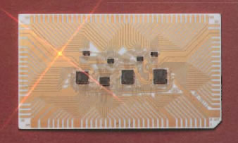
At the time the 9845A was designed, it was more or less a matter of philosophy whether to apply a flat addressing scheme (like later the 68000 did), a memory scheme with segments and offset (as it was implemented by the 8086), or a block-oriented scheme like the 9845 MAE. Today we prefer the flat scheme, mainly in order to avoid the artificial limitations and workaround complexity for large binary objects, but the MAE scheme with its access controlled automatic block selection mechanism had its appeal.
Memory Installation
Memory can be installed by different assemblies. In the 9845A, ROMs were generally provided as pluggable ROM modules, which had to be installed in one of the two ROM drawers. This changed with the 9845B/C, where the system ROMs with the OS and the BASIC interpreter were placed on an internal ROM/RAM assembly, and the ROM drawers were only used for ROM extensions (so-called option ROMs).
R/W memory was in the 9845A mounted on memory boards with 8 KBytes and 16 KBytes, whereas in the 9845B and 9845C there was a minimum amount of DRAM on the ROM/RAM boards of 64 KBytes and 32 KBytes. Both the 9845A and the 9845B/C were designed to expand the LPU R/W memory only by additional R/W memory boards. The 9845A was expandable to 64 KBytes LPU R/W memory, whereas the 9845B/C was expandable first to 448 KBytes and later to 1.5 MBytes.
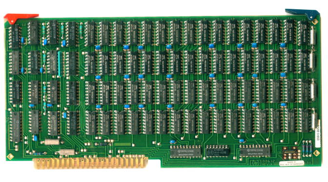
128K RAM Expansion Board (P/N 09845-66526)
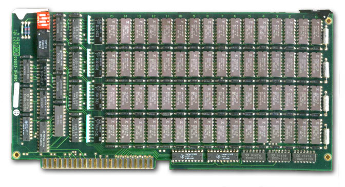
512K RAM Expansion Board (P/N 09845-66590)
The memory boards used different standard DRAM chips from several manufacturers. The 9845A used 4104 4Kx1 SRAMs for all memory assemblies, the 9845B used sixteen 4116 16Kx1 DRAM chips for the PPU RAM/ROM assembly, thirty-two 4116 for the LPU RAM/ROM assemblies, sixty-four 4116 16Kx1 DRAMs for the 128 KByte expansion board and sixty-four 4164 64Kx1 DRAMs for the 512 MByte expansion boards.
During start-up all memory is checked for usable DRAM, and the result is written into the block descriptors at the upper end of each R/W memory block. The available R/W memory is used dynamically during the execution of user programs.
Memory Map
Not much is known about the 9845 firmware structure. For the 9825 the situation is completely different since there is a commented assembler listing of the firmware code. Nothing comparable is public for the 9845, however many concepts of the 9825 were transferred and re-used for the 9845, so the 9825 firmware at least provides some hints for the 9845 firmware. In can be assumed, that for the 9845 not every part of the code was done in assembler, and it is very likely that HP's high-level system implementation language SPASM also was involved.
What we know is that the firmware was split into routine packages, represented by the names of the source code files. And from the 9845A patent document we also know the locations of those packages for the 9845A. In contrast to the firmware, the locations of the different usage areas in the R/W memory generally are not fixed, but held in special pointer variables (many locations depend on the amount of RAM installed).
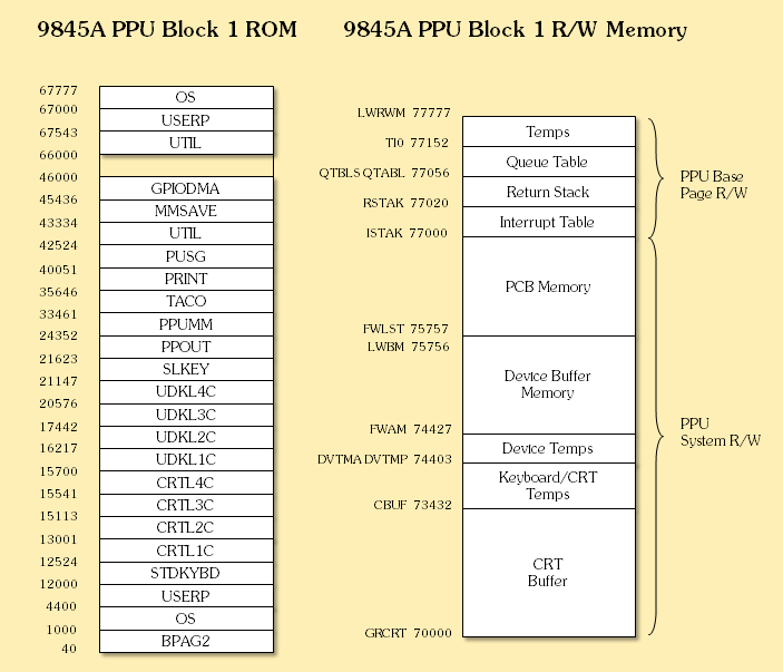
PPU Block 1 (combined firmware and R/W memory, 9845A only)
The PPU of the 9845A used only one single memory block for both firmware and R/W memory. This memory block could also be accessed by the LPU.
The LPU firmware is located in memory block 3 and occupies the whole 32 kWords except the 1.5 kWord space between octal 70000 and 76000, which is reserved for option ROM. The names of the routines in the diagram below refer to the names of the related source code files.
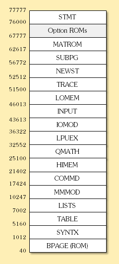
LPU Firmware Block 3 (9845A only)
Thanks to the Memory Address Extension, the LPU of the 9845A could gain access to all four memory blocks, including the PPU RAM/ROM block 1. Block 0 was intended for programs and system R/W memory, whereas block 3 was used for the LPU system firmware (mainly the BASIC interpreter) and one option ROM. Block 2 was completely reserved for additional option ROMs.
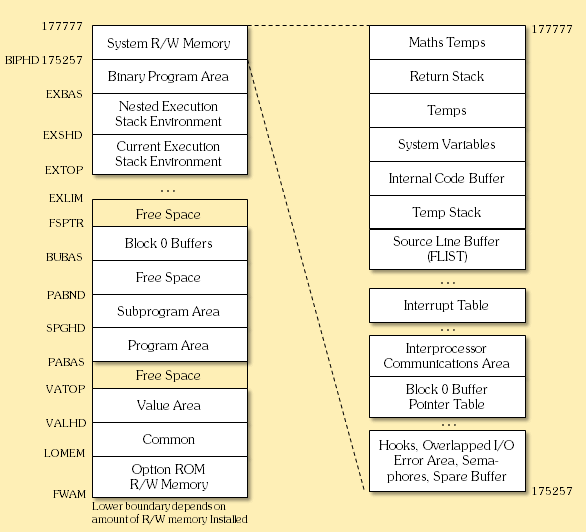
LPU R/W Memory Block 0 (9845A only)
Thanks to the patent document, the 9845A memory structure is better described than the memory use of the 9845B/C. Nevertheless, at least some information for the 9845B/C can be derived from the service manuals.
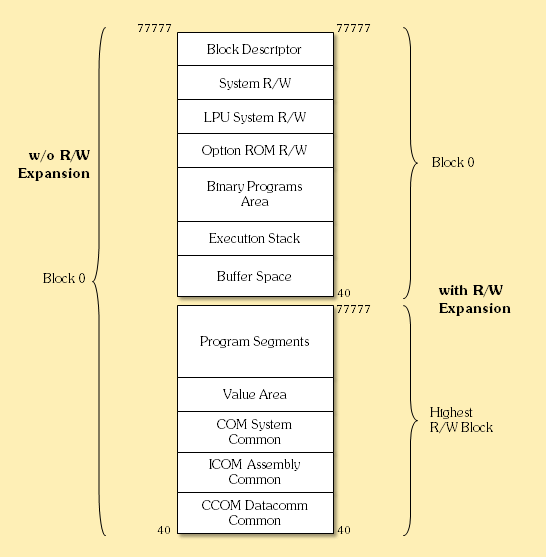
LPU R/W Memory (9845B/C only)
The above diagram shows two different memory address assignments, depending on whether the LPU is restricted to the minimum amount of R/W memory (one single 64 kByte memory block), or whether expansion RAM is installed. If only the basic amount of R/W memory is available, all areas have to fit into one memory block. If additional RAM is installed, the lower areas like the CCOM, the ICOM and the COM regions are moved to the highest available R/W memory block. The Block Descriptor holds some information about how much (working) physical memory is actually available in each memory block.
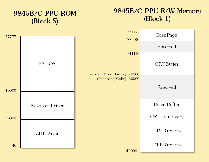
PPU Memory (firmware and R/W memory, 9845B/C only)
Note that the lower 32 words are always reserved for the internal processor and MAE registers. The CRT display buffer is used as shared memory and accessed by both the processors and the alpha display logic. Note also that the standard monochrome display buffer is located at address 70000 and the enhanced monochrome and the color display buffer at address 60000.
The Bus System
Just like modern PCs, the 9845 had two bus systems, one for the connections between the processor and memory (similar to the front side bus of modern dual-core pentiums), and another for the connections between the processor and the I/O system (today comparable to the PCI bus). Actually, there was an additional bus system not visible to the user, which connects the chips on the ceramic substrate with each other (the internal IDA bus).
The memory bus was designed slightly different for the 9845A and the 9845B/C. In the 9845A, memory blocks 0 and 1 were accessible by both the LPU and the PPU via a dual-port memory controller. This was necessary, because the PPU firmware, the CRT buffer and some PPU system R/W memory (including device buffers) was located in block 1, whereas inter-processor-communication memory, LPU system memory, programs and data buffers were located in block 0. Block 2 (LPU option ROMs) and block 3 (LPU system firmware) were hidden for the PPU and only accessible by the LPU.
Later with the 9845B/C the memory bus design became completely symmetrical, giving access to all memory areas for both the PPU and the LPU. The memory bus system was divided into two separated segments, the X bus, where the LPU ROM and R/W memory is connected, and the Y bus for connection of the PPU ROM and R/W memory. If you consult Tony Duell's schematics, he has called the X bus the L bus and the Y bus the P bus. Normally, each processor is connected through a bus switch to its own memory bus segment. Once an access to the other segment is required (e.g. for accessing the shared inter-processor communication memory), the bus switch is set to connect to the other processor's memory bus segment. Both bus segements have their own bus controller.
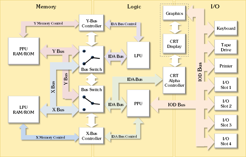
9845 B/C Bus System Overview
Each bus segment can handle ~1 million memory cycles per second, so the bus bandwith is somewhat around 2 MBytes/s. The alpha video circuit is directly connected to the PPU's fron side bus in order to periodically read out the video buffer content and transfer it to the CRT display. Bus arbitration for this purpose is done through the alpha video controller circuit and consumes up to 9% (worst case) of the PPU memory bus cycles.
The processor front side bus was also called the IDA (Instruction Data Address) bus, because both instructions and data were transferred through this bus, with address multiplexing on the same signal lines. So the memory bus had 16 address/data lines and a couple of bus control lines mainly for bus arbitration, address/data handshake and memory refresh. Actually the memory bus was just an extension to the processor internal IDA bus.
| Mnemonic | Description | Comments | |
| IDA0/ to IDA15/ | Memory Bus | Memory bus lines for 16-bit (word) or 8-bit (byte) data transfer. | |
| 01/, 02/ | Clock 1 & 2 | Clocks the memory bus, 02/ is 01/ inverted. | |
| RAL | Register Access Line | High for memory cycles involving register access (addresses 0 to octal 37). | |
| RDW | Read/Write | Specifies direction of data transfer (low is processor to memory). | |
| STM/ | Start Memory | Initiates a memory cycle, indicating that the contents of the IDA bus lines is an address. | |
| DSTM/ | Start Memory (Delayed) | Same as STM, but with one clock delay. Seems to be abandoned with the 9845B/C. | |
| UMC/ | Unsynchronized Memory Complete | Concludes a memory cycle. Set by the respondent to acknowledge that data has been put on the bus or read from the bus. | |
| SMC/ | Synchronized Memory Complete | Concludes a memory cycle. Set by the respondent to acknowledge that data has been put on the bus or read from the bus. Seems to be abandoned with the 9845B/C. | |
| BR/ | Bus Request | Request control of the IDA bus (either by the processor or other instances on the bus like the alpha video control). | |
| BG | Bus Grant | Indicates the bus request is agreed, however the originator has to wait for the EXBG/EBG signal before accessing the bus (see EXBG/EBG below). BG is precondition for any bus arbitration. All connected instances have to agree by setting this signal high. As long as this signal is grounded by any device, no bus release will occur. | |
| EXBG, EBG | Extended/External Bus Grant | Generated by IOC on BG going high and passed to all other instances via daisy-cain. Used to provide prioretized IDA bus arbitration to IOC, BPC, EMC and external devices. After a device has issued a bus request by setting BR/ low, it has to wait for this signal before any bus access is possible. | |
| SYNC | Instruction Fetch Synchronization | Set high by the processor during an instruction fetch memory read cycle. | |
| ERA/ | Extended Register Access | Not completely clear. Maybe a way to access the hidden internal registers. | |
| PDR/ | Processor is Driving | Indicates the current phase of the memory cycle is driven by the processor. Will cover the either a whole memory write cycle or the address phase of a memory read cycle. Seems to be abandoned for the 9845B/C. | |
| RELA | Relative Adressing | Switch processor to relative page addressing instead of absolute page addressing (relative is fixed). Seems to be abandoned for the 9845B/C (probably internally grounded). | |
| PBO/ | Processor Buffer Out | IDA bus drivers direction control. | |
| PBE/ | Processor Buffer Enable | Enable IDA bus buffers (normally driven internally). | |
| BYTE/ | Byte | Indicates a memory cycle involving a byte instead of a word. | |
| BL/ | Byte Left | Selects left (low) or right (high) half of the word as valid data. | |
A memory bus cycle is performed with the following steps:
- Initiator puts the appropriate address on the bus and sets the RDW line either high (read access) or low (write access)
- Initiator starts a memory bus cycle with setting STM/ low
- Responder reads address and checks whether he is involved within one memory clock phase
- Either initiator (write access) or responder (read access) puts data on bus
- For write access, responder first reads the data and then gives acknowledge by setting SMC/ or UMC/ low, for read access responder puts data on the bus and then sets SMC/ or UMC/ low
- For read access, initiator reads data from bus within one memory clock phase
In contrast to the memory bus, the I/O bus was reserved for the PPU only (in fact the LPU, although providing the signal lines for the I/O bus, was not even connected to this bus). As a consequence, all I/O communication could be performed by the PPU alone. If the LPU wanted to send data to a peripheral device, it had to hand it over to the PPU first.
| Mnemonic | Description | Comments |
| IOD0/-IOD15/ | I/O Data Bus | Transfers 16-bit data words between processor/memory and device. Is used during an I/O read or write cycle, i.e. when accessing to R4 to R7 or when performing an interrupt poll. |
| PAB0/-PAB3/ | Peripheral Address Bus | Addresses device or interface via device select code 0 to 15. Is set via the peripheral address register Pa. |
| IC1/, IC2/ | I/O Control | Provides additional information to the device or interface (device dependent, normally a register address). Is set automatically when accessing the peripheral I/O registers R4 (IC1=0, IC2=0) to R7 (IC1=1, IC2=1). By setting both lines to logical 1 the processor informs the device that the interrupt has been served and another interrupt may be issued (done by machine code "STA R7" or BASIC command "OUTPUT <select code>,7" ). During DMA transfers, the IOC automatically sets IC1 high during the I/O bus cycle for the last data word, which indicates the end of the current DMA block transfer to the device. |
| FLG/ | Flag | Information flag from the device or interface to the processor (if set, normally indicates the device is ready to transmit or receive data). The flag information can be retrieved either with an SFS or SFC machine instruction, or with an IOFLAG() BASIC function. |
| STS/ | Status | Status flag information from the device or interface to the processor (if set, normally indicates the device needs some service, e.g. out of paper). The status information can be retrieved either with an SSS or SSC machine instruction, or with an IOSTATUS() BASIC function. |
| DC/ | Decimal Carry | Decimal carry flag. For the 9845A, this line is used for indicating vertical retrace for the PPU. For the LPU or the 9845B/C PPU, this flag is driven by the EMC indicating an arithmetic overflow condition. |
| HLT/ | Halt | Halt flag. For the 9845A, this line is driven low by CONTROL-STOP. For the 9845B/C, this line is used for indicating vertical retrace for both processors. |
| INIT/ | Initialize | Sends reset signal to all I/O devices or interfaces. |
| INT/ | Interrupt line | Used by the processor to initiate an interrupt poll sequence and to cause the processor to execute "JSM 10B,I" (indirect subroutine jump to interrupt vector). |
| IRH/ | Interrupt Request (high priority) | Used by the device or interface to request high priority interrupt service. This line will be used for devices with select codes between 8 and 15. The line will be hold low by the device until the interrupt has been served. |
| IRL/ | Interrupt Request (low priority) | Used by the device or interface to request high priority interrupt service. This line will be used for devices with select codes between 0 and 7. The line will be hold low by the device until the interrupt has been served. |
| DMAR/ | DMA Request | With setting this line low, a device or interface requests a DMA transfer from the processor. |
| DOUT/ | Data Direction | Direction of I/O data transfer, set by the processor (low means data from processor to a device or interface). |
| BE/ | I/O Buffer Enable | Enable IOD bus buffers (normally driven internally). |
| IOSB/ | I/O Strobe | This signal is set low by the processor during an I/O read or write cycle for indicating to the device or interface that there is valid data on the I/O bus. |
The I/O bus was also called the IOD (I/O Data) bus. In contrast to the IDA bus, there was no addressing on the IOD bus, instead there is a separate bus, the peripheral address bus (PAB), consisting of address lines PAB0 to PAB3, through which one of up to 16 devices can be addressed. Two additional lines, the IC1 and IC2, can be used to pass additional information to a device, e.g. for addressing up to four I/O registers directly.
The I/O System
The I/O system constists of the I/O processor (the PPU), the 16-bit I/O bus (the IOD bus), and I/O devices connected to the IOD bus either directly or via plugable interfaces.
Communication could happen either via programmed I/O, interrupts or DMA, just as with today's PCs. Since both DMA and interrupt controller were implemented into the processor, in fact all communication was between the processor and a device. Programmed I/O was done via four bi-directional I/O registers R4 to R7 and four address lines PA0 to PA3, so up to 16 devices could directly be addressed.
Some device addresses or "select codes" were reserved for special devices like 0 for the keyboard and the internal printer, 13 for the CRT graphics, 14 and 15 for the internal cartridge drives, or 16 for the CRT alpha display (actually a pseudo-device). All other addresses (1-12) could be freely assigned, however there were defaults for most interfaces, like 6 for the line printer, 7 for the HP-IB interface, 9 for the real-time clock and 10 for the RS232C interface, and the interfaces had to be re-configured via the select code switch in order to match select codes other than the defaults.
From the processor side, a device is addressed by writing the appropriate select code to the PA (peripheral address) register. Note that pseudo-devices (devices with select codes higher than 15) exist only at OS level and can't be addressed via the PA register.
Programmed I/O
The four registers were implemented into the processor, and each read or write access initiates an I/O cycle, transferring the content of the register to the register implementation in the device, or vice versa. Actually, each device could implement an arbitrary number of shadow registers, but all programmed data transfer to and from the devices was performed via the four registers R4 to R7. Accessing R4 automatically triggers the IC1 and IC2 lines to false, accessing R5 triggers IC1 to true and IC2 to false etc. So the device "knows", which register is to be to served.
Programmed I/O involves three activities:
- Setting the peripheral address (in the PA register)
- Investigating the status of the peripheral
- Initiating an I/O bus cycle (accessing one of the registers R4 to R7)
Programmed I/O was also used to setup the device for interrupts and/or DMA transfer.
Note that programmed I/O in most cases uses handshake with the device in order to transfer data, which is performed by doing a dummy write to R7 to tell the device that either the data word previously written into R4 is valid (output), or the current data word has been accepted by the host and the device can fetch the next data word into R4 (input).
I/O Interrupts
I/O interrupts are the most used mechanism for communication with devices. As long as there is no data to transfer, the processor is free for other processing tasks. But if there is data to transmit, the processor can immediately handle that request without any delay, which is very useful especially for real time processing of instrument data, but perfect as well for more trivial tasks like processing key strokes.
The basic principle is that whatever the processor is doing, if a device signals that data is ready for transfer, the processor interrupts its current task, branches into an appropriate handler routine, reads or writes the data as needed, and, when processing is finished, returns back exactly to where the processor was interrupted and proceeds with that task just as if there would have been no break.
Technically, the interrupt mechanism is implemented in the I/O chip, the IOC. It uses the IRL, IRH and INT lines plus PAB3 and the I/O data lines for handshake. A device signals an interrupt request by setting IRL or IRH low, depending on whether the select code of the device is in the range 0-7 (low priority) or 8-15 (high priority). Now the IOC knows there is a request, but does not know from which device. So it initiates an I/O cycle with INT line low, which signals an interrupt poll towards all devices connected to the IOD bus. Also, the PAB3 line is set according to the interrupt level received. During this poll, the device which requested the interrupt sets one of the lines IOD0 to IOD7 low according to its own select code modulo 8.
Now the IOC can determine which device(s) originated the interrupt request and decide which device to serve. The select code of the device being served will be pasted into the lower four bits of the interrupt vector (IV) register at address octal 10 and written into the PA register, saving the previous value of the PA register onto an internal stack. Now the BPC is triggered to perform an two-level indirect subroutine jump to the address stored in the IV register (while the INT line is still low) which branches into the appropriate interrupt handler via a vector table previously prepared by the system firmware. While the state of the interrupt is kept in the IOC, the INT line will then be reset high before the next instruction fetch is performed (thus terminating the interrupt poll and re-enabling single-level indirection).
Of course interrupts can happen while the processor is already processing an earlier interrupt. in order to prevent the processing of more critical interrupts from being interrupted by less important interrupts, two interrupt priorities or levels can be used.
Generally, interrupts may or may not be served, there is no guarantee that an interrupt requested by a device will be granted. The IOC implements a simple scheme: If the processor is in normal processing and there is no ongoing interrupt, the interrupt request is granted. If a low-level interrupt is being served, only high-level interrupts will be granted. In case a high-level interrupt is active, all interrupt requests are ignored until the interrupt has been handled.
The IOC uses a three-entry-stack to keep track of the select codes. The current select code is always in the PA register, which builds the top of the stack. Previous select codes, which are active when the interrupt request happens, will be automatically saved for each granted interrupt and re-stored on a first-in last-out base after the interrupt handler has finished. Due to the depth of three, the stack can track three select codes, which allows two nested interrupts plus one 'normal processing' select code.
There is no acknowledge for the device that an interrupt request has been granted. So it is up to the interrupt handler to inform the device about being served, e.g. by initiating an I/O cycle.
Interrupt priority depends on the interrupt line used (IRH for high level interrupts and IRL for low level interrupts). Just for the case that two interrupts of the same level happen at the same time, the select code of the device is used for the decision which interrupt is to be processed (the higher the select code, the higher the interrupt priority). All other interrupt requests are being ignored.
The addresses of the interrupt routines are held in a 16-word jump vector table in R/W memory. The table must start on a 16-word boundary. Each entry denotes the address of the interrupt handler routine for a specific select code. The address of this table is written into the IV register (interrupt vector) at the address octal 10, so that the processor knows where to branch to.
Depending on the response of the interrupt poll, the lower four bits of this register are set to the select code of the device which requested the interrupt, so that execution can be directed to the proper interrupt handler via a two-level indirect subroutine jump (JSM plus INT line low) to the IV register. It is then the responsibility of the interrupt handler to save all register contents, flags or memory locations which may be altered through the routine and to restore them before exiting from the handler with an RET operation. The two-level indirection is a specialty of the BPC which is only active when the INT line is low. It is not yet quite clear how the IOC gets knowledge about when the interrupt handler has finished (in order to update its interrupt state counter).
Normally, interrupts are triggered by the device either when a device wants to send data, or is ready to receive data, or just has changed its status (e.g. out-of-paper). All interrupts first have to be configured properly by the program (either the OS firmware or the BASIC program).
Please note that interrupts in BASIC are not the same as interrupts on system level, although they have a certain relation. Once an interrupt has occured on system level, it is handled by the appropriate system interrupt service routine. This interrupt service routine decides whether the interrupt should be reported further to BASIC or not. At the time when a BASIC line execution has finished, the interpreter looks whether one of the interrupts which had been enabled with an ON INT instruction has been reported, checks for the priority of this interrupt and branches to the BASIC routine which handles the interrupt with the highest priority. This BASIC level interrupt handling mechanism is also referred to as "end of line branch".
So, although on system level only two interrupt levels are supported, BASIC can differentiate 15 interrupt levels. Note also that BASIC handlers with ON INT ... GOTO always run on priority level 0 (allowing any other interrupt to intercept execution) and BASIC handlers with ON INT ... GOSUB or ON INT ... CALL run with the same priority level as the causing interrupt (allowing only interrupts with higher priority level to intercept execution before the RETURN statement has been reached).
Under some conditions, it may not be appropriate to allow interrupts, e.g. during time critical processing. In that case all system level interrupts may be inhibited by using the DIR (disable interrupts) and re-enabled by the EIR (enable interrupts) machine instructions.
Direct Memory Access (DMA)
Direct memory access is a mechanism for directly writing from a device into memory (i.e. into a buffer previously pepared by the program which initiates a DMA transfer), bypassing the processor and all its processing overhead. Ideally, a DMA transfer can happen while the processor can do other things in parallel.
The 9845 system implements two different mechanisms for DMA. The first one is called "memory cycle stealing" and is used by the alpha display logic for access to the refresh memory in PPU R/W memory block 1. This type of DMA is performed directly via the IDA bus and is not part of the I/O system. The other DMA mechanism belongs to the I/O concept and as such works over the IOD bus with the PPU's IOC as intermediate DMA controller.
In general, the I/O DMA process has priority over the display DMA, with the effect, that during burst DMA disk transfers the display may be temporarily be blanked.
The basic procedure for performing an I/O DMA transfer is
- Setting up the three DMA registers (Dmapa, Dmama and Dmac) for the pripheral address, the buffer address, the DMA word count and setting the the transfer direction with either an SDI or SDO machine instruction
- Sending a (device specific) DMA start command to the device via programmed I/O, if possible with (again device specific) information about the number of words to be transferred.
After the start command has been issued, everything else is done between the DMA controller (built into the IOC chip) and the device. Each word transfer (in either direction) is initiated by the device by setting DMAR/. The IOC then performs a bus request on the IDA bus, and manages the exchange between system memory and the device, totally independent of the remaining system operation, except stealing memory cyclyes.
DMA progress can be monitored through reading the Dmac register, which is automatically decremented with every word transfer. Depending of the capabilities of the device, notification at the end of a DMA transfer can be signalled via interrupt. In the other direction, the DMA controller sets IC2/ on the last word to be transferred while IOSB/ is asserted (for all other word transfers, IC1/ and IC2/ are automatically cleared by the IOC during DMA), so the device can terminate the DMA transfer even if it doesn't know the word count in advance.
The DMA transfer speed which is supported by the IOC should be theoretically around 400 kWords/second or 800 kBytes/second. The effective DMA transfer speed normally is limited by the peripheral interface, which is somewhat below, depending on the speed of the connected device. The 98032 16-bit GPIO interface supports up to 200 kWords/second. One of the fastest transfers should be that between the frame buffer of the graphics subsystem and the main system memory, which should approximate to the maximum during horizontal/vertical blank periods. Same applies to the 98041 disk interface connected to a 7906 or 7920 hard disk, which are specified with 937 kBytes/second maximum transfer rate which are probably not fully available for the 9845 because of DMA speed limitations.
DMA can generally be disabled with the DDR and re-enabled with the DMA machine instructions.
The main prerequisites for using DMA are that
- the device has to be capable for performing DMA transfers, and
- the single DMA channel (yes there is only one) is not already in use by another DMA transfer.
Actually, beyond the graphics subsystem there are only two interfaces supporting the I/O DMA transfer method, the 98032 16-bit parallel GPIO interface (which is mostly using DMA for talking to the 9885 floppy disk drive) and the 98041 disk interface. So the standard application for I/O DMA transfers actually is mass storage data transfer.
DMA transfers are a matter of machine language device drivers, there is no direct DMA control in BASIC. However the I/O ROM ENTER and OUTPUT commands can be used with the DMA option to request DMA transfers.
The CRT Display
The 9845 CRT display is directly connected to the mainframe through a digital interface without any intermediate cable. This makes monitor positioning a bit less flexible compared to a standard PC (monitor position is fixed). Moreover, the connection interface is completely proprietary, so it isn't possible to connect anything but an HP 9845 monitor. All video signals are generated inside the monitor, the interface to the computer is completely digital, comparable to DVI in contrast to VGA.
The display system consists of four parts:
- the alpha memory buffer,
- an alpha control assembly,
- a graphics subsystem and
- a CRT monitor system.
The display system can operate in two modes, the alpha mode and the graphics mode.
For more information on the 9845 displays please have a look at the CRT Displays section.
The Human Interfaces
The 9845 concepts includes a couple of input devices. Supported are
- the keyboard (including a numeric keypad and a set of special function keys),
- soft-keys built into the monitor (98770A and 98780A only),
- digitizer hardware,
- grapics tablets, and
- light-pens.
The computer mouse was already invented (since 1972), but still used more or less inside the labs of Xeroc PARC. Nevertheless, the 9845 was too much oriented towards technical applications requiring precise control, that even a joystick was part of the human interface concept. However, it wouldn't be a real problem to connect a serial mouse to a 98036A RS232C interface anyway. See the Mouse Project Section on how that can be done.
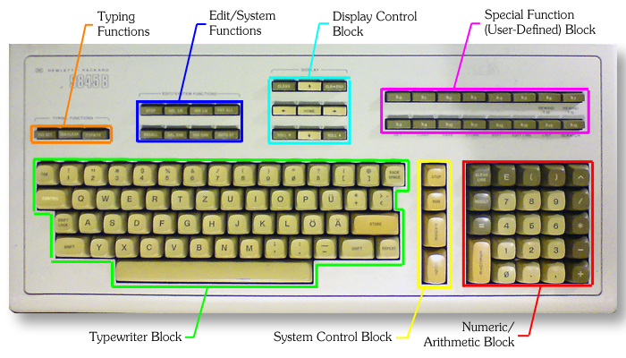
9845 Keyboard (German Layout)
The keyboard was connected internally to the IOD peripheral data bus. The 9874A digitizer hardware and the 9111A graphics tablet both were connected via the standard peripheral bus, the HP-IB bus. The light-pen required a special controller board installed in either a 98780A enhanced monochrome monitor and a 98770A color monitor.
HP delivered six different keyboard languages, English (standard ASCII), French, Spanish, German, Katakana and Swedish/Finnish. The alphanumeric and symbol key layout for both the standard US and foreign keyboards was derived from the popular IBM Selectric typewriters (some kind of industry standard at the time) and is quite close to the IBM PC keyboard layout.
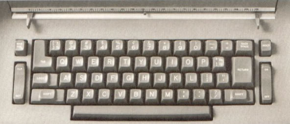
IBM Selectric Keyboard
A special issue was that for foreign keyboard layouts, some characters which were needed for programming (especially the '[' and ']' brackets) were not available on the top row. HP solved this problem partly by simply adding those characters to the shifted upper row of the numeric keypad. However, I could not yet manage to produce '{' and '}' braces on a German keyboard, also there is no way to produce single quotes.
Some keys could be latched (SHIFT LOCK, PRT ALL, AUTO ST), whereas others had two levels (arrow keys), one for normal operation and one for auto-repeat. In general, auto-repeat could be switched on for all keys by pressing the REPEAT key. Key mechanics were of high quality - even after more than 30 years there are almost never contact problems with the key switches themselves. Also, even compared to modern keyboards, fast typing still is easy with those keyboards.
The light-pen was a real technical challenge, since most light-pens before were operated with vector displays, not with raster displays.
The Mass Storage Concept
The 9845 as a desktop computer didn't have a virtual memory implementation as it could be found on the larger machines. However there was a variety of mass storage options which could be used to persistantly store and exchange programs and data, including tape, floppy disk and winchester storage.
The standard mass storage medium was the DC100 tape cartridge. It could hold up to 213 kBytes and transfer data with an average data rate of 1,440 bytes/sec. There was one standard (select code 15) and one optional tape cartridge drive (select code 14), both internally connected to the I/O system via the IOD peripheral data bus.
The next most common mass storage was the 9895A 8" dual floppy disk drive, holding up to 1,155 kBytes on each floppy disk. Older, but still common was the 9885M 8" floppy disk drive with up to 458 kBytes storage. The 9895A was connected to the 9845 mainframe through HP-IB, the 9885M via a 98032A GPIO interface.
There was a couple of larger hard disk drives (both fixed and removable), and one winchester drive, which all were compatible with the 9845 system. Directly supported were
- the 7905M, 7906M, 7920M and 7925M disk drives, requiring a 98041 disk interface, and
- the 7908, 7911P and 7912P disk drives and the 7910H winchester drive, all requiring an HP-IB interface.
A special case were the 9133A, 9134A and 9135A winchester drives, which could be used with the 9845 systems in a 9895A emulation mode.
The whole mass storage firmware design was based on a principle called unified mass storage concept. The idea was, that all mass storage operations were generic and implemented mostly independent from the specific mass storage used. This was a renunciation from the previous principle of assuring media compatibility over a variety of systems. However, though cutting compatibility with other systems, the unified mass storage concept vastly simplified the use of mass storage. Most applications needed just the change of one single line of code (the "MASS STORAGE IS" is statement) in order to run with another mass storage device. And even network drives could easily be configured and used (see the next section).
The single drawback was that each specific mass storage needed its own driver as part of the PPU firmware. So new drivers needed firmware upgrades or new option ROMs. It was not possible to "load" any driver dynamically e.g. for connecting newer mass storage devices. Unfortunately, even those devices with standardized communication protocols like the AMIGO or the CS/80 protocol could only be used as long as the specific hardware was already known by the firmware. Which indeed was a really unnecessary restriction, at least as far as it concerns the CS/80 protocol which provided means to query all relevant drive parameters.
The Networking Concept
Yes, the 9845 was a networking system (as it used to be as our very first workstation system). However, networking wasn't too common at the time, and this feature actually was introduced at a time when the next generation workstations, the 98x6 technical desktops, were already available. Nevertheless, with the Shared Resource Management (SRM) network, there was everything a workstation needs: servers, nodes, network printers and and a network file system.
Thanks to the unified mass storage concept mentioned above, the use of network storage was completely transparent for the 9845.
The SRM network was built around a 9826/9836 as a server, and required a special SRM interface for connecting the 9845 to the SRM (the 98029A Resource Management interface), plus a special Resource Management option ROM set.
Of course, there were less sophisticated and less extensive networking solutions, like terminal or file transfer connections. See the Tutorials section for more information.
Connectors
I/O and Memory Expansion Connectors
Peripherals are connected to the 9845 mainframe via so-called interface modules. Interface modules are responsible for translating between the system I/O bus (the IOD bus) and the peripheral interface. Just like the expansion boards of a modern PC they plug into the system I/O bus via edge connectors, from where they are connected to the data and control lines of the IOD bus as well as to the power supply. In contrast to PCs, the modules are not installed inside the mainframe, but can be easily plugged in and removed at the rear of the mainframe without the need to open it.
Each interface module consists of one or two PCBs inside of a standardized plastic housing which can be fixed into any free I/O slot with a snap-in machanism. In order to distinguish the interface modules, each interface module has an address switch, through which it can be assigned a unique ID, the so-called selection code. All interface modules connect to the peripherals via a suitable cable and connector (in fact, those interfaces look much more like cables than like expansion boards). Actually, there is one interface module, the Real Time Clock module, which doesn't necessarily connect to a peripheral device. Some of the interface modules are really complex devices and contain their own microprocessor, for example the 98046B datacomm interface is a small computer with its own 8048 microcontroller, and both the 98034A/B and the 98035A use HP's own Nanoprocessor.
Below on the left is a diagram of the signals at the I/O expansion slot.
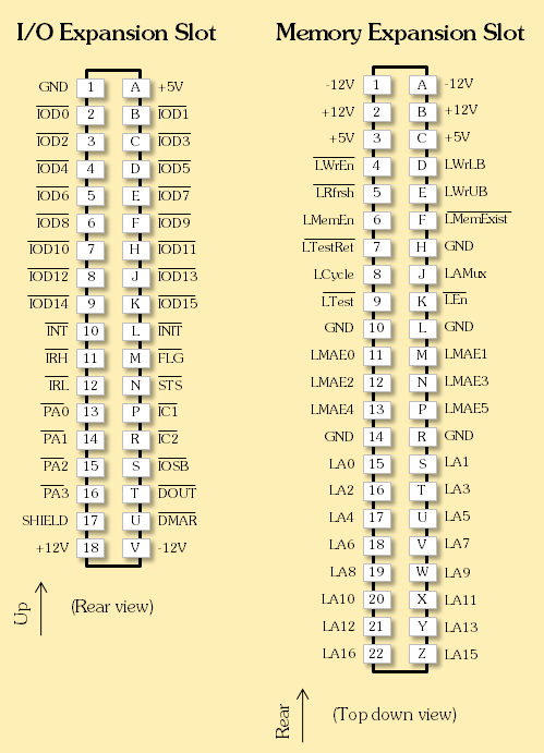
All memory expansion boards are installed inside the mainframe on the left side next to the PPU processor board. They are directly connected to the LPU's IDA bus with its 16-bit data bus and its control lines, as well as to the memory extension lines MAE0 to MAE5 for block addressing. See the right side of the diagram above for the assigment of the memory expansion slots. The signal names refer to those which are used by Tony Duell in his schematics.
Option ROM Drawer Connectors
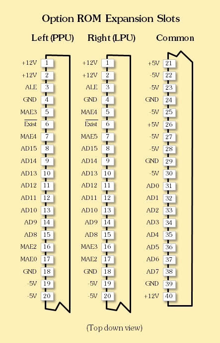
Option ROMs are means to extend the firmware of both the LPU and the PPU. They are enclosed in standardized modules as one to eight 1K x 16-bit ROMs and can be installed in one of the two ROM drawers by the user without the need to open the mainframe. The left ROM drawer is dedicated for extensions of the PPU firmware, the right ROM drawer for extensions of the LPU firmware. Bot drawers differ slightly in their address line layout. Below is a diagram which shows the specific part of the PPU drawer module slots on the left, the specific part of the LPU drawer module slots in the middle and the common assignment on the right, mostly referring to the signals names which are used by Tony Duell in his schematics.
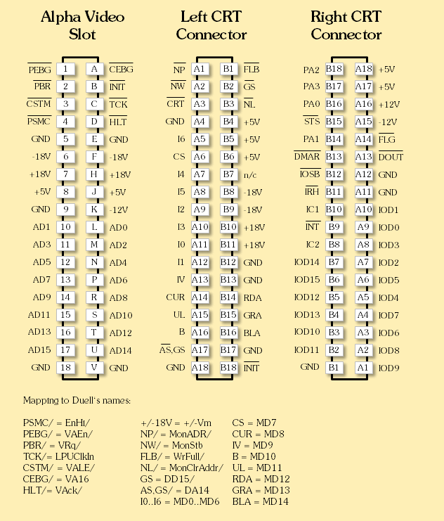
CRT Display Connectors
The display is connected to the mainframe through two edge connectors inside the two display legs. Below the display legs are on the left side the alpha controller board (which is again connected to the IDA bus on the mainboard via the alpha video slot), and on the right side the graphics interconnect board, which passes the IOD bus signals from the mainboard through to the graphics subsystem of the monitor. Both legs also transport different voltages from the mainframe to the CRT display.
In principle, the interfaces are the same for all 9845 systems, however some of the signals are not used by the standard monochrome monitor (graphics select and color information) or the enhanced monochrome monitor (color information). Probably the alpha video slot on the 9845A uses the DC (decimal carry) signal instead of the HLT (halt) signal. The signals are named according to the service manuals, an appropriate mapping to the names Tony Duell uses in his schematics is included.
Other connectors like the internal keyboard, printer or tape drive connectors are probably not as important as the ones diskussed above, however if you need some information about those connectors, please refer to Tony Duell's schematics of the 9845B.
Power Supply (PSU) Connectors
The power supply unit is directly connected to the mainboard via two edge connectors, one with 44 contacts for the main logic and CRT voltages, and another with 20 contacts for tape and printer voltages.
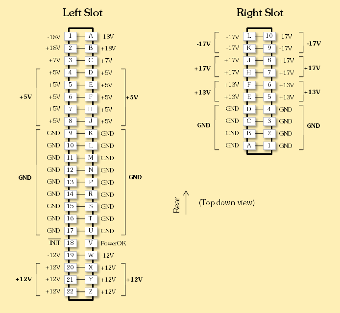
PSU to Mainboard Connectors
Note that the edge connector slots on the mainboard are often subjects to stress, caused time wear in combination with the force from the weight of the PSU. It is highly recommended not to ship a 9845 system with PSU installed, but rather to remove the PSU before shipping, and to pack mainframe and PSU separately.
The Assemblies
The whole 9845 computer was a highly modular system. One of the drawbacks is, that there are almost no repair service information other than how to exchange complete assemblies ("board swapping"). Nevertheless, the 9845 already incorporated a variety of modern concepts like thermal design, air flow channels, expansion slots for both system upgrades and peripheral interfaces, as well as CRT display, mass storage and printer integrated into a nice, robust and serviceable industrial design, which was cutting-edge at the time and exemplary for later workstations and personal computers.
For more information on the 9845 assemblies please have a look at the Assemblies section.
Thermal Design
Not many systems of the time had the high integration level of the 9845 systems. Since many features were packed into a comparably compact desktop design (well, compact with respect to the fridge-sized cabinets which were common for the more performent systems of the time), the produced heat had to be carried out of the system. Several components have been equipped with die-cast heat sinks, like the processors, the tape controller or the PSU regulators. Cool air is pulled through two air-filter ports beneath the keyboard and guided through four air channels towards two fans in the rear of the mainframe, where the warm air is moved outside.
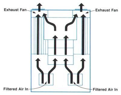
9845 Air Flow
Both types of monochrome CRT monitors are completely passive-cooled just by convection and the use of heat sinks. The color monitor needs two fans to transport the heat of nearly 500 Watts outside the monitor, which makes the 9845C significantly more noisy than a 9845B. The nominal operating noise level of the 9845B with standard monochrome monitor is 46 dBA.
Industrial Design
The design of the 9845 is, like many things, more or less a matter of taste. At the time of the 9845, the computer design wasn't as uniform as it is today with all those IBM compatibles. Today's vivid case modding scene or the success of Apple's current products is one indicator for the desire to break out this tedious situation. In the late 70's, industrial design was an important part of a product strategy, so form and function built a unit.
But back to the 9845. Responsible for the industrial design was Leroy LaCelle, who previously did design the 9825. There is a great article about his work on HP9825.com (follow this link). Also there is a design patent for the 9845 (see the Patents section). The colors chosen for the case were a bit typical for the time. The official color tones were "cocoa brown" and "pearl grey", plus a third yellowish color for the most used keys which appears also on some of the manual cover sheets. For the attentive reader, it will not have escaped his notice that this site has been designed with this color scheme in mind. The manual binders themselves were held in the same "pearl grey" as the system. The system's case is actually of foam-molded grey pastic, covered with a conductive shielding inside and with the "pearl grey" and "cocoa brown" outside.
What was really exemplary for later designs was how a CRT terminal design was combined with the desktop computer housing. It looked very futuristic and although it had two times the size of the later Apple II (still my personal favorite concerning industrial design), the highly complex system fitted well on a desktop. Actually, the 9845 was one of the very first systems really looking like a modern computer.
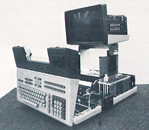 Another concern is the user and service friendlyness of the design.
For the user, all important functions are at hand, no cables disturb the desktop, since all connections are at the back of the system. The keyboard is quite applicable for fast typing. All ROM and I/O expansions could be done by the user without opening the case. Transportation was facilitated by a detachable CRT and carrying cases.
For the service, once the upper case and the keyboard screws are removed, everthing inside the mainframe was directly accessible. The Keyboard could be tilted upside down for free access to the keyboard and tape drive assemblies. Most units could be removed from the system and exchanged within minutes, including the complete PSU.
The monitors are highly ergonomic, even the smaller standard monochrome CRT provides a flickerless 60Hz image with sharp high-definition characters with true ascenders and descenders in a 9x15 cell (at the time, 8x8 was standard for home computers). The standard monochrome monitor had an anti-glare coating and a 5-degree negative tilt in order to reduce reflections from the overhead lighting. The effort on the color monitor in achieving perfect color convergence with 39 potentiometers was outstanding.
More Information
Most system architecture information can be derived from the 9845B/C Service Manual, the 9845B/C CE handbook and, of course, the patent documents. The processor block functions can be examined in the 9845A patent, whereas the 9825 patent contains logic details for the implementation of the BPC, the IOC and the EMC. The manuals can be downloaded from HPMuseum, as well as Tony Duell's perfect 9845B schematics, and the patents are available here. In addition, there is a good overview including lots of details in the arcticle from the McGraw-Hill publication "Computer Structures: Principles and Examples" (look here for download) and in the April 1978 issue of the HP Journal (which can be downloaded here). For information concerning the hybrid processor, including many historical references and comments, visit the HP9825.COM website.
