RAM Repair
RAM is one of the most essential resources in any computer, and the 9845 has lots of it. Steve Wozniak, the inventor of the Apple computer, once said that it was alleged in Silicon Valley that the microprocessor was invented to sell programmable and read only memory chips. Most HP 9845 systems have more than 100 DRAM chips, so the chance is relatively high that some of those are running into defects through the decades.
Typical symptoms for R/W memory defects are printouts on the internal printer during power-up, error messages during the initial start-up memory test ("PART OF MEMORY FAILED SELF-TEST!") and less memory reported by the LIST command than 'officially' installed. Also, repeatedly beeping (about once per second) after start-up can be an indication for a memory fault.
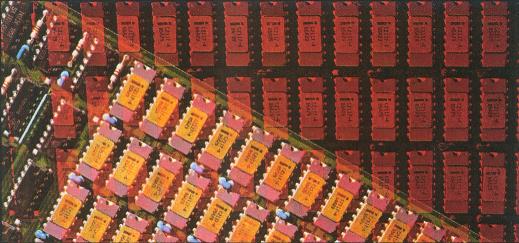
In fact, repair of faulty DRAMs is no rocket science. Here is what you need:
- A small side cutter and pliers or tweezers
- A low-power soldering iron with de-soldering tool (e.g. solder sucker) and some electronics solder and soldering flux
- A memory exerciser program (e.g. from the System Exerciser tape) for diagnostics
- Some (good) spare DRAM chips of the appropriate type (4116 or 4164)
The steps for performing RAM repair are always the same:
- First, it has to be identified whether the fault is in fact related to memory and if yes, whether it is caused by the address decoder logic, the refresh logic or an individual DRAM chip.
- Next, the affected memory assembly has to be identified.
- Then the faulty component on the assembly has to be found.
- The component has to be replaced, and finally
- an exerciser should be run to verify the cause has been successfully eliminated and the system has regained 100% operation.
R/W Memory Organization
Note that all the R/W memory in the HP 9845 is organized in blocks of 64 kBytes or 32 kWords, except block 1, which is only 32 kBytes or 16 kWords of RAM. Memory is dedicated to one of the system's processors, but can be accessed by both via a cross switch circuit. In general, all R/W memory is assigned to the LPU and to even block numbers, except block 1, which is assigned as system RAM to the PPU. The highest possible R/W block address is octal 76. The maximum amount of RAM which can be installed in an HP 9845 is 1,632 kBytes or 1.6 MB.
Most essential for operation are blocks 0 and 1, since they are used directly by the operating system and option ROMs for buffers and variables. Block 1 also holds the CRT alpha buffer starting at octal address 70000 (model 100) or 60000 (model 200).
All R/W memory is implemented with dynamic RAM (DRAM) chips. All assemblies are using 4116 chips, except for the 98047A 512k Option RAM assembly which uses 4164 chips.
32 kWord memory blocks can be mapped to the processor's 64k address space either using the lower half of the address space (octal 000000 to 077777) or using the upper half of the address space (100000 to 177777). Since the processor's registers are mapped to octal 000000-000040, this range can't be directly accessed as R/W memory. For testing this portion of R/W memory, it has to be mapped to address 100000-177777. Mapping is controlled by the MAE registers (R32 to R37) and configured in software.
All R/W assemblies for the HP 9845 can be configured to different block addresses via jumper or DIP switch. The RAM/ROM assemblies which are holding both the ROMs and the system RAM for each of the two processors can be configured to block 0 or 1. The 128k option RAM assembly can be configured to blocks 0+2, 4+6, 10+12 and 14+16. The 512k option RAM assembly can be set to blocks 20-36, 40-56 and 60-76.
In principle, it is possible to use an A28 LPU RAM/ROM board as replacement for an A27 PPU RAM/ROM board. Both differ only in that the A28 has both rows of DRAM chips installed, whereas the A27 has only the upper row populated with DRAMs. So when the block select jumper is set to block 1 (PPU setting), the A28 board can safely be used as A27 board. The additional RAM will simply not be used. Using an A27 in turn as replacement for an A28 obviously is not possible, unless you solder in the missing DRAM chips.
R/W Memory Diagnostics
You need the memory exerciser in order to identify the bad DRAM chip(s). There are four different exercisers available for the HP 9845B/C (all information below refers to those models):
- The most common exerciser is part of the test suite from the exerciser tape. Simply load the tape or mount the exerciser disk image with HPDrive, load and run the AUTOST program and select the MEMORY test.
- Another possibility is to do the same with the test binary program (TBIN), which also can be loaded and run from tape or from a mounted disk image. Among the test options, choose Memory Troubleshooter.
- The third option to run a memory exerciser is to use the 9845 Test ROM, which also provides a basic memory test, but which only tests the LPU and PPU system RAM on the A15 and A16 RAM/ROM assemblies.
- Finally there is a built-in memory test which is integrated in the system startup routine and as such executed automatically on each power-up sequence. The informative value of this test is limited, and it needs a working internal printer setup for its output, however it is the only built-in test procedure which is always available. In fact this test is primarily intended to identify the amount of memory usable for the system, rather than providing comprehensive diagnostic information.
Which exerciser to use depends partly on which memory assembly is affected. If the system boots up and a tape can be loaded or disk image mounted, the test suite from the exerciser suite probably is the best choice, since it features the most comprehensive memory tests.
If the system does not boot up (probably because the system LPU and/or PPU RAM fails), you need the Test Option ROM. Actually this special Option ROM is an extremely rare item, so I have included the Test ROM code in the current ROM set for the ROM board (a replacement for the system ROMs, see the ROM Board Project Section).
If the system does not boot up and you don't have either the Test ROM or a ROM board for using the Test ROM code from flash memory, you still can try to interpret the output of the start-up memory test.
The test binary program features almost the same memory diagnostics as the exerciser tests, but can be loaded directly from the Test ROM and so can be used even when many of the other system components fail and so the exerciser tape can't be loaded. The test binary's memory troubleshooter offers selecting individual test routines, including memory refresh tests, walking 1s tests, and a peek/poke function, and so can be used with focus on special types of problems.
Except the start-up memory verifier, all tests return error information the same format, so that the following steps towards component identification and repair are the same. In the following section, the four different diagnostic procedures are described step by step. Just choose the one you want to use, work it through step by step, and then proceed with the section Intepreting R/W Memory Error Information.
Using the System Exerciser Tape
Every HP9845 delivered had a tape cartridge called 'System Exerciser' with it. The exerciser was primarily intended for the user himself to assure he has a fully operational system. So there is not too much to configure and the procedures are easy to execute. For every functional area of the system, there is a dedicated exerciser, including interfaces and peripherals.
See the System Utilities Section for downloading the System Exerciser.
To perform the memory diagnostics, follow these steps:
- Power-up the system
- Load the System Exerciser tape cartridge into one of the internal tape drives or mount the System Exerciser hpi disk image file with HPDrive
- Execute LOAD "AUTOST" and press RUN when load is completed
- Tell the program whether you need printed output for retaining full logs (internal printer has select code 0)
- Type MEMORY at the prompt and press CONT
In fact the MEMORY exerciser first tests the ROM checksums ("ROM CHECKSUM TEST RUNNING"), and then starts testing the installed read/write memory ("R/W MEMORY EXERCISER RUNNING") from the uppermost memory block down to block 0:
NOW TESTING BLK BB 000000-037777
NOW TESTING BLK BB 040000-077777
It takes about one minute to test each block. You should not interrupt this test by pressing any key, however you always can terminate the test with pressing STOP. The last block which will be tested by the exerciser is block 1. Note that testing block 1 will result in strange patterns on the screen, this is normal.
Once finished, the exerciser will display
MEMORY EXERCISER COMPLETE, PRESS "CONT"
Since the memory test destroys all data in memory, the system must be restarted after the test is completed.
If a R/W memory error is found, this test indicates the failure by the message:
MEMORY ERROR BLK BB ADDRESS AAAAAA HAS XXXXXX NOT YYYYYY
Now proceed with the section Intepreting R/W Memory Error Information.
Using the Test ROM
The Test ROM does an automatic memory test for the system memory blocks 0 (LPU) and 1 (PPU). Note that block 0 has a full memory block installed (64 kBytes) with the address range octal 000000 to 077777, whereas block 1 has only 32 kBytes installed with the address range 040000 to 077777.
To perform the memory diagnostics, follow these steps:
- Install the Test Option ROM in the PPU ROM drawer (the one to the left), or, alternatively set the DIP-switch on the ROM board to position 7 (Test ROM)
- Power-up the system
Now the system automatically tests first the PPU, then the LPU. After those tests have finished successfully, system memory blocks 0 and 1 are tested. During the tests, the currently tested memory block is indicated by
BLK 0 SA - 000040 EA - 077777 or
BLK 1 SA - 040000 EA - 077777
It takes about one minute to test each memory block. You should not interrupt this test by pressing any key, however you always can terminate the test with pressing STOP. The last block which will be tested by the exerciser is block 1. Note that testing block 1 will result in strange patterns on the screen, this is normal. Also note that only blocks 0 and 1 are tested, so this test is not suited for testing user memory at blocks 4 and above.
Once finished, the exerciser will display
**** PRESS SFK-KEY TO START A TEST *****
The memory test can be re-launched from here as desired with the K9 key.
If a R/W memory error is found, this test indicates the failure by the message:
LPU MEM ERR BLK BB ADDR AAAAAA HAS XXXXXX NOT YYYYYY or
PPU MEM ERR BLK BB ADDR AAAAAA HAS XXXXXX NOT YYYYYY
The LPU or PPU in this case indicates, which processor has performed the memory test. Normally, defect DRAMs should be reported by both processors. If not, this can be an indication for bad processor or bus paths rather than for defect R/W memory.
Now proceed with the section Intepreting R/W Memory Error Information.
Using the Test Binary Program
The test binary program was originally meant in combination with the Test Option ROM for on-site diagnostics performed by the service personnel. It includes a memory troubleshooter with four memory tests and a peek/poke function. You can load and start the test binary program either from the Test ROM, or from BASIC.
Since you can individually select the tests to be performed, you also can check different types of failures. See the System Utilities Section for downloading the test binary program (TBIN).
To perform the memory diagnostics, follow these steps:
- Power-up the system
- Load the test binary program either from the Test ROM (e.g. by pressing the K8 SFK-key) or from BASIC with LOAD BIN "TBIN"
- After loading is completed, the test binary will be automatically executed. Select K8 - MEMORY TROUBLESHOOTER from the test menu.
- Now select the indivdual exerciser you want to run. Press M and then CONT for marching pattern test.
- Press A to test all memory blocks
The memory test will start testing PPU system block 1, and then all other installed R/W memory blocks starting at block 0 up to block 16 (note that 98407A 512k-assemblies are not tested):
MEMORY TEST BLK BB 000000-037777
MEMORY TEST BLK BB 040000-077777
It takes less than 20 seconds to test each block. The whole test will run continously until STOP is pressed. You should not interrupt this test by pressing any other key. Note that testing block 1 will result in strange patterns on the screen, this is normal.
If you like, you can repeat this test with the selection of R (for refresh test), B (for byte test) or W (for walking bit test) instead of M. Note that the walking bit test take about six hours to test each memory block.
If a R/W memory error is found, this test indicates the failure by the message:
MEMORY ERROR BLK BB ADDRESS AAAAAA HAS XXXXXX NOT YYYYYY
Now proceed with the section Intepreting R/W Memory Error Information.
Using the Start-up Memory Test
The startup memory test is the least thorough test and only does a quick check on the memory. However every memory block installed will be tested.
To perform the memory diagnostics, follow these steps:
- Load some thermal paper into the internal printer (you can use standard fax thermal paper for this)
- Power-up the system
During the test, the message "MEMORY TEST IN PROGRESS" will be displayed. If there is no error during start-up, the message "9845 READY FOR USE." is shown. If the system can boot up despite of memory errors, finally "PART OF MEMORY FAILED SELF-TEST!" will be displayed on the screen.
For understanding the start-up memory test you have to consider that the LPU R/W memory (all even memory blocks) is divided into eight sub-blocks of 4 kWords (8 kBytes) each.
There are two types of tests performed, one type which I call full address test, where all memory addresses are tested until the first error is found, and another type I call quick test, since only the first word of each 4k word sub-block is tested top-down. The memory test starts with a full address test at PPU system memory block 1, and continues with a quick test on LPU memory block 0 up to the uppermost memory block installed.
If a memory error is detected during a full address test, an error message is printed and no further testing is performed on this block (or sub-block). If a memory address fails during quick test, or if it is found that no memory is installed at this address, the sub-block where the error occurs and all sub-blocks below are considered as unusable and will not be further tested.
After the quick test of the LPU R/W memory has been completed, all LPU memory marked as usable will be tested bottom-up with full address tests starting at the first sub-block in block 0. If there is a memory error detected in a sub-block, an error message is printed and test continues with the next higher sub-block. So, effectively, only one error message will be printed if there is bad RAM in block 1, and only one error message will be printed for any bad RAM detected in each sub-block. See the Troubleshooting Tutorial for detailed information on the system start-up procedure and the built-in memory test.
If the memory test fails on certain memory addresses, there will be an output to the printer in the form:
0000BB AAAAAA XXXXXX
Now proceed with the following section Intepreting R/W Memory Error Information. With some luck, you can use the information for identification of the bad DRAM chip.
Interpreting R/W Memory Error Information
Once one of the memory exercisers described above has found an error, it will be listed so that four information types are reported (all numbers are octal):
BB is the memory block address, where the error has been detected
AAAAAA is the memory address in this block where the error occured
XXXXXX is the (faulty) data which has been read, and
YYYYYY is the data which would have been expected if there had been no fault
Now all this information combined can be used to identify the assembly and the chip which is responsible for the error as follows:
-
First determine which memory assembly contains the block indicated by BB in the error message. Refer to the following table for help:
Block Assembly DRAM TypeBlock 0: A28 LPU RAM/ROM Assembly (09845-6528) 4116Block 1: A27 PPU RAM/ROM Assembly (09845-66527) 4116Blocks 4-16: A26 128 kByte LPU Option RAM Assembly (09845-66526) 4116Blocks 20-76: 98407A 512 kByte LPU Option RAM Assembly (09845-66590) 4164
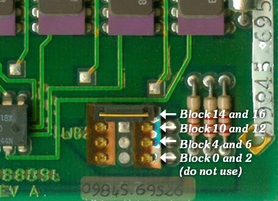
A26 (09845-66526) Block Address Selection
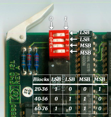
98407A (09845-66590) Block Address Selection
- Use the address infomation AAAAAA as hint whether the upper half or the lower half of a block is affected:
a) If AAAAAA is below 040000, lower half of a block is indicated (lower chip row)
b) If AAAAAA is 040000 or above, upper half of a block is indicated (upper chip row)
Note that this information is not needed for the 98407A 512k board. Also note that if the error information is from a test with the built-in start-up memory test, for technical reasons all addresses will begin with a 1 as first digit, which should be treated as 0. - Decode the XXXXXX and YYYYYY data into binary values and compare the bits:
Actual data XXXXXX: 0 000 000 100 000 000 Expected data YYYYYY: 0 000 000 000 000 000
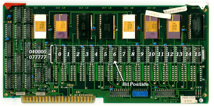
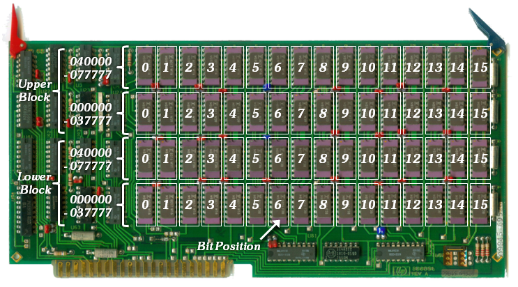
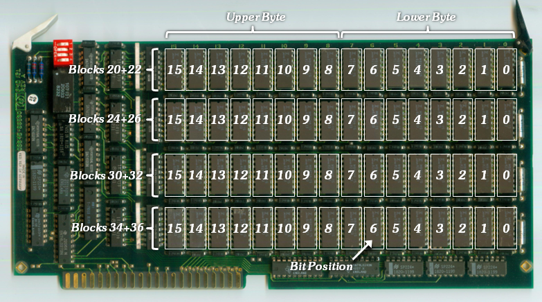
Special comment on the start-up memory test: If you got the error information from this test, there is no 'expected' YYYYYY value. You have to check on your own, whether the XXXXXX value reported by the test should be compared to 177777, 125252 or 052525 (these are the patterns used by the start-up memory test, simply compare to the value which is closest to the XXXXXX value). Also note that - due to the way the start-up memory test is implemented - a memory failure can result also in an XXXXXX value which is exactly one of the test patterns. In that case, it is not possible to identify the individual faulty DRAM chip, you only can try to repeat the test and hope that you get a different result. - The bits that do not compare indicate a defective RAM location. The following illustrations show the DRAM chips that correspond to each bit position:
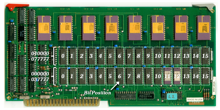
A28 LPU RAM/ROM Assembly (Memory Block 0)
A27 PPU RAM/ROM Assembly (Memory Block 1)
A26 128 kByte LPU Option RAM (Memory Blocks 4-16)
98407A 512 kByte LPU Option RAM (Memory Blocks 20-76)
The information described here has been derived from the Memory Troubleshooter section on page 4-10 ff. in the 9845B/C CE Handbook, or on page 2-25 in the HP 9845B/C Desktop Computer Service Manual.
Example
Imagine the HP 9845 during system boot outputs "MEMORY TEST IN PROGRESS" on the screen and
000000 170000 117777
on the internal printer, and then hangs. The message suggests that an error is found when testing block 0 at address 070000 (note the first address digit is always 1 and should be treated as 0). Block 0 is on the A28 LPU RAM/ROM assembly, and the address 070000 indicates the upper half of the block is affected. So the bad chip oviously is located in the upper chip row of the A28 (09845-66528) assembly.
Next, the the value read 117777 should be compared to one of the patterns used in the start-up memory test. Obviously, the expected value would be 177777, so the comparison works out to
1 001 111 111 111 111 (actual value) vs.
1 111 111 111 111 111 (expected value)
^^
which suggests that bits 13 & 14 are affected. So the chips to be replaced would be #13 & #14 in the upper row on the A28 09845-65528 assembly. At this point we have some luck, since the value read differs from the expected value. For the built-in start-up memory test this unfortunately is not always the case.
Now we try the same, but with the Test ROM as exerciser. The first error message can be for example
LPU MEM ERR BLK 0 ADDR 040030 HAS 020000 NOT 000000
Again, the indicated memory block is block 0. The address 040030 shows that the upper half of this block is affected, because it is an address above 037777. The actual value of 020000 compares to the expected value as
0 010 000 000 000 000 (actual value) vs.
0 000 000 000 000 000 (expected value)
^
Here, only bit 13 does not compare, so we at least know that we have to replace chip #13 in the upper row on the A28 09845-65528 assembly. In fact, this had been a real example where chips #13 & #14 in the upper row, and chip #14 in the lower row had to be replaced. The Test ROM exerciser can be continued after an error, which in this case will show that more chips are bad when using different test patterns.
In general, if more than one chip is affected, the defective chips have to be replaced one after the other, and will be detected finally when one chip is replaced and the excerciser is run again.
DRAM Replacement
Replacing defect DRAMs is a comparably easy task. Once the bad chip has been identifed, just follow these steps:
- Remove the defective chip form the board by cutting all pins with the side cutter
- Use some soldering flux paste on the back side of the PCB so that de-soldering of the pins gets easier
- De-solder the pins one after the other
- Use the de-soldering tool to clean the solder points
- Solder in the replacement chip (check for proper chip orientation). If you like you also can solder in sockets, however take into account there is limited space between the PCBs in the mainframe)
Take care not to overheat the solder points, since they may otherwise get off the PCB. Also, the new DRAM chip is sensitive to both static electricity and overheating.
Repair Verification
After you have replaced the bad chip(s), you should run the memory exerciser again in order to verify the repair had been successful and whether there are more defective chips left which also have to be replaced.
When everything seems ok with the exerciser of your choice, you should run the final test with the memory test from the System Exerciser tape cartridge over a longer period of time (say one hour) on the memory block which has been repaired. If everthing work out well, congratulations, you have successfully revived your R/W memory.
More Information
Most information on this page has been derived from the Memory Troubleshooter section on page 4-10 ff. and 5-12 ff. in the 9845B/C CE Handbook, or from the Memory Section on page 2-19 ff. in the HP 9845B/C Desktop Computer Service Manual. Both documents can be downloaded from the HP Museum at www.hpmuseum.net.